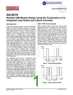
AN-8019
APPLICATION NOTE
The rectangular current pulses represent a worst-case
condition to ensure the power supply design works well at
the GSM/GPRS modem load. To meet this pulsed load
condition, there are several areas a designer should consider
in GSM/GPRS wireless modem designs based on a USB
input source. First, the power supply should not overload the
self-powered USB hub’s limited power specification.
Although the power specification is 5V and 500mA, there
seems to be some margin at current supplying capacity
because most USB hubs in the market can provide up to 1A
to cover variable portable applications downstream. Second,
a DC/DC step-down converter should cover the periodic 2A
pulse load conditions with limited input current. In addition,
it should regulate the 3.6V output required by most power
amplifiers. Finally, the appropriate reservoir output
capacitor should be placed in front of the power amplifier to
supply pulsed current during transmission.
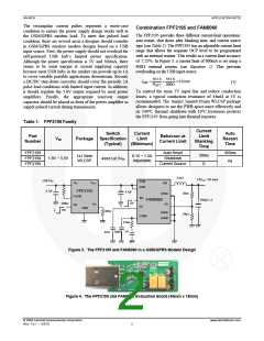
Combination FPF2195 and FAN8060
The FPF2195 provides three different current-limit operations:
auto-restart, shut down after blanking time, and current source
type (see Table 1). The FPF2195 has an adjustable current limit
range that allows the requisite OCP level to be programmed
with an external resistor. This results in a current limit accuracy
of ±25%. In Figure 3, a current limit of 600mA is set using a
900Ω external resistor (see Equation 1). This prevents
overloading on the USB input source.
551.6 551.6
I
=
=
= 612mA
(1)
LIM
R
900Ω
SET
To control the main 5V input line and reduce conduction
losses, a typical conduction resistance of 44mΩ at 5V is
recommended. The 1mmx1.5mmx0.65mm WLCSP package
allows designers to use the PWB space more effectively and
its 140°C thermal shutdown with 10°C hysteresis protects
the FPF2195 from going into thermal runaway.
Table 1. FPF2195 Family
Current
Switch
Package Specification
(Typical)
Current
Limit
(Minimum)
Auto
Restart
Time
Part
Number
Behavour at
Current Limit
Limit
Blanking
Time
VIN
FPF2193
FPF2194
FPF2195
Auto Reset
Shutdown
450ms
na
30ms
0
1x1.5mm
0.15 ~ 1.5A
Adjustable
1.8V ~ 5.5V
44mΩ at 5VIN
WLCSP
Current Source
3.3µH
3.6VOUT / PA Input
USB 5VIN
PVIN
AVIN
VIN
VOUT
SW
4.7µF
FPF2195
FLAGB
4.7µF
20kΩ
SYNC
EN
SS
1500µF x 2
FAN8060
EN
100kΩ
ISET
FB
ON
0
GND
ON
0
900Ω
PGND
AGND
10kΩ
COMP
8.2kΩ
1nF
100pF
82nF
Figure 3. The FPF2195 and FAN8060 in a GSM/GPRS Modem Design
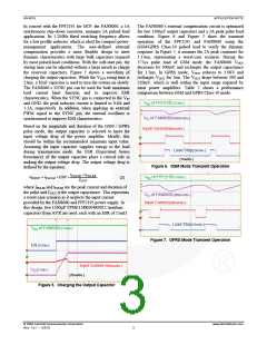
Figure 4. The FPF2195 and FAN8060 Evaluation Board (40mm x 18mm)
© 2009 Fairchild Semiconductor Corporation
Rev. 1.0.1 • 5/3/10
www.fairchildsemi.com
2

 FAIRCHILD [ FAIRCHILD SEMICONDUCTOR ]