XRT86L30
SINGLE T1/E1/J1 FRAMER/LIU COMBO
REV. 1.0.1
F
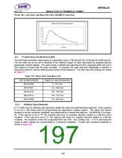
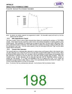
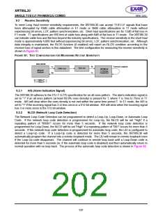
IGURE 55. ARBITRARY
P
ULSE
S
EGMENT
ASSIGNMENT
1
2
3
4
Segment
Register
1
2
3
4
5
6
7
8
0x0F08
0x0F09
0x0F0a
0x0F0b
0x0F0c
0x0F0d
0x0F0e
0x0F0f
8
7
6
5
NOTE: By default, the arbitrary segments are programmed to 0x00h. The transmitter outputs will result in an all zero
pattern to the line interface.
8.3.2
DMO (Digital Monitor Output)
The driver monitor circuit is used to detect transmit driver failures by monitoring the activities at TTIP/TRING
outputs. Driver failure may be caused by a short circuit in the primary transformer or system problems at the
transmit inputs. If the transmitter of a channel has no output for more than 128 clock cycles, DMO goes "High"
until a valid transmit pulse is detected. If the DMO interrupt is enabled, the change in status of DMO will cause
the interrupt pin to go "Low". Once the status register is read, the interrupt pin will return "High" and the status
register will be reset (RUR).
8.3.3
Transmit Jitter Attenuator
The transmit path has a dedicated jitter attenuator to reduce phase and frequency jitter in the transmit clock.
The jitter attenuator uses a data FIFO (First In First Out) with a programmable depth of 32-bit or 64-bit. When
the Read and Write pointers of the FIFO are within 2-Bits of over-flowing or under-flowing, the bandwidth of the
jitter attenuator is widened to track the short term input jitter, thereby avoiding data corruption. When this
condition occurs, the jitter attenuator will not attenuate input jitter until the Read/Write pointer’s position is
outside the 2-Bit window. In T1 mode, the bandwidth of the JA is always set to 3Hz. In E1 mode, the
bandwidth is programmable to either 10Hz or 1.5Hz (1.5Hz automatically selects the 64-Bit FIFO depth). The
JA has a clock delay equal to ½ of the FIFO bit depth.
NOTE: The Receive Path has a dedicated jitter attenuator. See the Receive Path Line Interface Section.
187

 EXAR [ EXAR CORPORATION ]