Document No.: FT_000288
FT232H SINGLE CHANNEL HI-SPEED USB TO MULTIPURPOSE UART/FIFO IC
Datasheet Version 1.8
Clearance No.: FTDI #199
Appendix A – List of Figures and Tables
List of Tables
Table 3.2 Common Function pins.................................................................................................. 10
Table 3.3 EEPROM Interface Group ............................................................................................... 11
Table 3.4 UART Interface and ACBUS Group (see note 1) ................................................................ 12
Table 3.5 ACBUS Configuration Control ......................................................................................... 13
Table 3.6 UART Configured Pin Descriptions................................................................................... 14
Table 3.7 FT245 Synchronous FIFO Configured Pin Descriptions ....................................................... 15
Table 3.8 FT245 Style Asynchronous FIFO Configured Pin Descriptions.............................................. 16
Table 3.9 Synchronous or Asynchronous Bit-Bang Configured Pin Descriptions ................................... 17
Table 3.10 MPSSE Configured Pin Descriptions ............................................................................... 18
Table 3.11 Fast Serial Interface Configured Pin Descriptions............................................................. 19
Table 3.12 CPU-style FIFO Interface Configured Pin Descriptions ...................................................... 20
Table 3.13 FT1248 Configured Pin Descriptions .............................................................................. 21
Table 4.1 FT245 Synchronous FIFO Interface Signal Timings............................................................ 28
Table 4.2 Asynchronous FIFO Timings (based on standard drive level outputs)................................... 29
Table 4.3 Synchronous Bit-Bang Mode Timing Interface Example Timings.......................................... 35
Table 4.4 MPSSE Signal Timings................................................................................................... 36
Table 4.5 Fast Serial Interface Signal Timings ................................................................................ 38
Table 4.6 CPU-Style FIFO Interface Operation Select....................................................................... 41
Table 4.7 CPU-Style FIFO Interface Operation Read Status Description.............................................. 41
Table 4.8 CPU-Style FIFO Interface Operation Signal Timing. ........................................................... 42
Table 4.9 Configuration Using EEPROM and Application Software ...................................................... 46
Table 5.1 Absolute Maximum Ratings ............................................................................................ 47
Table 5.2 Operating Voltage and Current (except PHY).................................................................... 48
Table 5.3 I/O Pin Characteristics VCCIO = +3.3V (except USB PHY pins)........................................... 49
Table 5.4 PHY Operating Voltage and Current................................................................................. 50
Table 5.5 PHY I/O Pin Characteristics ............................................................................................ 50
Table 5.6 ESD Tolerance.............................................................................................................. 50
Table 6.1 OSCI Input characteristics ............................................................................................. 54
Table 7.1 Default External EEPROM Configuration ........................................................................... 57
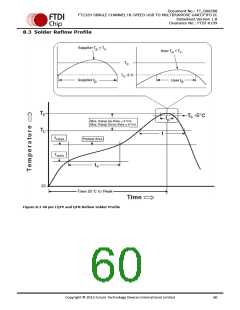
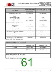
Table 8.1 Reflow Profile Parameter Values ..................................................................................... 61
Table 8.2 Package Reflow Peak Temperature.................................................................................. 61
Copyright © 2012 Future Technology Devices International Limited
63

 ETC [ ETC ]