EFST
F49L004UA / F49L004BA
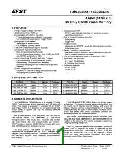
4. PIN CONFIGURATIONS
4.1 40-pin TSOP I
A17
40
1
A16
A15
A14
A13
A12
A11
A9
VSS
39
2
N C
38
3
N C
37
4
A10
36
5
DQ7
35
6
DQ6
34
7
DQ5
33
8
A8
DQ4
32
9
WE
RESET
N C
RY/BY
A18
A7
VCC
31
10
11
12
13
14
15
16
17
18
19
20
VCC
30
N C
29
DQ3
28
DQ2
27
DQ1
26
A6
DQ0
25
A5
OE
24
A4
VSS
23
A3
CE
22
A2
A0
21
A1
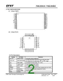
4.2 32-pin PLCC
4
3
2
1 32 31 30
A14
A13
A8
2 9
2 8
2 7
2 6
2 5
2 4
2 3
2 2
2 1
5
6
7
8
A7
A6
A5
A9
A4
A11
OE
A3
9
A2
10
11
12
13
A10
CE
A1
A0
DQ7
DQ0
14 15 16 17 18 19 20
4.3 Pin Description
Symbol
A0~A18
Pin Name
Address Input
Functions
To provide memory addresses.
To output data when Read and receive data when Write.
DQ0~DQ7
Data Input/Output
The outputs are in tri-state when OE or CE is high.
To activate the device when CE is low.
To gate the data output buffers.
Chip Enable
Output Enable
Write Enable
Reset
CE
OE
To control the Write operations.
WE
Hardware Reset Pin/Sector Protect Unprotect (for 40-TSOP)
RESET
Ready/Busy
To check device operation status(for 40 TSOP)
To provide power
RY/ BY
VCC
Power Supply
Ground
GND
Elite Flash Storage Technology Inc.
Publication Date : Sep. 2003
Revision: 1.0 2/46

 ESMT [ ELITE SEMICONDUCTOR MEMORY TECHNOLOGY INC. ]