EFST
F49L004UA / F49L004BA
Reset Mode :
Hardware Reset (for 40-TSOP package)
valid addresses on the device address inputs produce
valid data on the device data outputs. The device remains
enabled for read access until the command register
contents are altered.
See “Read Command” section for more information.
Refer to the AC Read Operations table for timing
specifications and to Figure 5 for the timing diagram. ICC1
in the DC Characteristics table represents the active
current
When the
pin is driven low for at least a
RESET
period of tRP, the device immediately terminates any
operation in progress, tri-states all output pins, and
ignores all read/write commands for the duration of the
pulse. The device also resets the internal state
RESET
machine to reading array data. The operation that was
interrupted should be reinitiated later once the device is
ready to accept another command sequence, to ensure
the data integrity.
specification for reading array data.
The current is reduced for the duration of the
RESET
is held at VSS±0.3V, the device
pulse. When
RESET
draws CMOS standby current (ICC4). If
Write Mode
is held
RESET
To write a command or command sequence (which
includes programming data to the device and erasing
at VIL but not within VSS±0.3V, the standby current will
be greater.
sectors of memory), the system must drive
and
CE
WE
to VIL, and
to VIH. The “Program Command” section
OE
The
pin may be tied to system reset circuitry.
RESET
has details on programming data to the device using
standard command sequences.
A system reset would thus reset the Flash memory,
enabling the system to read the boot-up firm-ware from
the Flash memory.
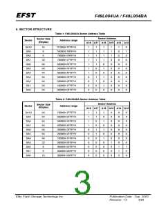
An erase operation can erase one sector, multiple
sectors, or the entire device. Tables 1 and 2 indicate the
address space that each sector occupies. A “sector
address” consists of the address bits required to uniquely
select a sector. The “Software Command Definitions”
section has details on erasing a sector or the entire chip,
or suspending/resuming the erase operation.
If
is asserted during a program or erase
RESET
embedded algorithm operation, the RY/
pin remains
BY
a "0" (busy) until the internal reset operation is
complete, which requires a time of tREADY (during
Embedded Algorithms). The system can thus monitor
RY/
to determine whether the reset operation is
BY
complete.
When the system writes the auto-select command
sequence, the device enters the auto-select mode. The
system can then read auto-select codes from the internal
register (which is separate from the memory array) on
DQ7–DQ0. Standard read cycle timings apply in this
mode. Refer to the Auto-select Mode and Auto-select
Command sections for more information. ICC2 in the DC
Characteristics table represents the active current
specification for the write mode. The “AC Characteristics”
section contains timing specification tables and timing
diagrams for write operations.
If
is asserted when a program or erase
RESET
operation is not executing , i.e. the RY/
reset operation is completed within a time of tREADY (not
during Embedded Algorithms). The system can read
data after tRH when the
Refer to the AC Characteristics tables for Hardware
Reset section.
is “1”, the
BY
pin returns to VIH.
RESET
Read Mode
Automatic Sleep Mode
To read array data from the outputs, the system must
The automatic sleep mode minimizes Flash device
energy consumption. The device automatically enables
this mode when addresses remain unchanged for over
250ns ns. The automatic sleep mode is independent of
drive the
and
pins to VIL.
is the power
CE
OE
CE
control and selects the device.
is the output
OE
control and gates array data to the output pins.
WE
the
,
, and
control signals. Standard
OE
WE
CE
should remain at VIH. The internal state machine is set
for reading array data upon device power-up, or after a
hardware reset. This ensures that no spurious
alteration of the memory content occurs during the
power transition.
address access timings provide new data when
addresses are changed. While in sleep mode, output
data is latched and always available to the system. ICC4 in
the DC Characteristics table represents the automatic
sleep mode current specification.
No command is necessary in this mode to obtain array
data. Standard microprocessor’s read cycles that assert
Elite Flash Storage Technology Inc.
Publication Date : Sep. 2003
Revision: 1.0
7/46

 ESMT [ ELITE SEMICONDUCTOR MEMORY TECHNOLOGY INC. ]