Page 8
Epson Research and Development
Vancouver Design Center
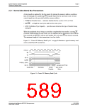
2 Interfacing to the MPC821
2.1 The MPC8xx System Bus
The MPC8xx family of processors feature a high-speed synchronous system bus typical of
modern RISC microprocessors. This section provides an overview of the operation of the
CPU bus in order to establish interface requirements.
2.2 MPC821 Bus Overview
The MPC8xx microprocessor family uses a synchronous address and data bus. All IO is
synchronous to a square-wave reference clock called MCLK (Master Clock). This clock
runs at the machine cycle speed of the CPU core (typically 25 to 50 MHz). Most outputs
from the processor change state on the rising edge of this clock. Similarly, most inputs to
the processor are sampled on the rising edge.
Note
The external bus can run at one-half the CPU core speed using the clock control register.
This is typically used when the CPU core is operated above 50 MHz.
The MPC821 can generate up to eight independent chip select outputs, each of which may
be controlled by one of two types of timing generators: the General Purpose Chip Select
Module (GPCM) or the User-Programmable Machine (UPM). Examples are given using
the GPCM.
It should be noted that all Power PC microprocessors, including the MPC8xx family, use
bit notation opposite from the convention used by most other microprocessor systems. Bit
numbering for the MPC8xx always starts with zero as the most significant bit, and incre-
ments in value to the least-significant bit. For example, the most significant bits of the
address bus and data bus are A0 and D0, while the least significant bits are A31 and D31.
The MPC8xx uses both a 32-bit address and data bus. A parity bit is supported for each of
the four byte lanes on the data bus. Parity checking is done when data is read from external
memory or peripherals, and generated by the MPC8xx bus controller on write cycles. All
IO accesses are memory-mapped meaning there is no separate IO space in the Power PC
architecture.
Support is provided for both on-chip (DMA controllers) and off-chip (other processors and
peripheral controllers) bus masters. For further information on this topic, refer to Section
6, “References” on page 22.
The bus can support both normal and burst cycles. Burst memory cycles are used to fill
on-chip cache memory, and for certain on-chip DMA operations. Normal cycles are used
for all other data transfers.
S1D13506
X25B-G-008-03
Interfacing to the Motorola MPC821 Microprocessor
Issue Date: 01/02/08

 EPSON [ EPSON COMPANY ]