Epson Research and Development
Page 7
Vancouver Design Center
13506CFG Configuration Tabs
13506CFG provides a series of tabs which can be selected at the top of the main window.
Each tab allows the configuration of a specific aspect of S1D13506 operation.
The tabs are labeled “General”, “Preference”, “Memory”, “Clocks”, “Panel”, “CRT/TV”,
and “Registers”. The following sections describe the purpose and use of each of the tabs.
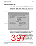
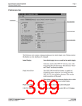
General Tab
Decode Addresses
Register Address
Display Buffer Address
The General tab contains S1D13506 evaluation board specific information. The values
presented are used for configuring HAL based executable utilities. The settings on this tab
specify where in CPU address space the registers and display buffer are located.
Decode Addresses
Selecting one of the listed evaluation platforms changes
the values for the “Register address” and “Display
buffer address” fields. The values used for each evalu-
ation platform are examples of possible implementa-
tions as used by the Epson S1D13506 evaluation board.
If your hardware implementation differs from the
addresses used, select the User-Defined option and
enter the correct addresses for “Register address” and
“Display buffer address”.
13506CFG Configuration Program
Issue Date: 01/03/14
S1D13506
X25B-B-001-02

 EPSON [ EPSON COMPANY ]