Epson Research and Development
Page 13
Vancouver Design Center
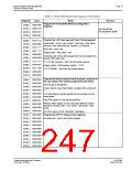
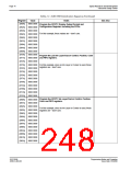
Table 2-1: S1D13506 Initialization Sequence (Continued)
Register
Value
Notes
See Also
Program the Frame Buffer Memory Configuration
Registers.
[020h]
[021h]
[02Ah]
[02Bh]
0000 0000
0000 0110
0000 0001
0000 0001
see REG[020h] -
REG[02Bh] for details
Program the LCD Panel type and Panel Timing Registers.
[030h]
[031h]
[032h]
[034h]
[035h]
[036h]
[038h]
[039h]
[03Ah]
[03Bh]
[03Ch]
0010 0110
0000 0000
0100 1111
0001 1111
0000 0000
0000 0000
1101 1111
0000 0001
0010 1100
0000 0000
0000 0000
Panel width = 16-bit; Color Format = don’t care; Color Panel
selected; Dual Panel selected; Passive LCD selected.
MOD rate = don’t care;
Display width = 640 pixels = 4Fh.
Horizontal and Vertical Non-display time has been adjusted to
provide 78Hz frame rate.
TFT FPLINE registers = don’t care for passive panels.
Display height = 480 therefore register = 1DFh
TFT FPFRAME = don’t care for passive panels.
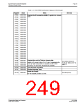
Program the Display Output Format and Start Locations for
the LCD output. This includes programming the FIFOs.
[040h]
[041h]
[042h]
[043h]
[044h]
[046h]
[047h]
[048h]
[04Ah]
[04Bh]
0000 0003
0000 0000
0000 0000
0000 0000
0000 0000
0100 0000
0000 0001
0000 0000
0000 0000
0000 0000
Select 8 bpp in REG[040h]
Ensure that the Dual Panel Buffer is enabled REG [41h] bit 0 =
0
LCD Start Address should typically be from location 0 in the
frame buffer.
Pixel Pan register is 0 for normal operation.
Memory offset register is set to ‘the panel width for normal
operation, therefore 640 ÷ 2 for words = 320 words= 140h
words
Set FIFO values to 0 for “automatic” calculation.
[050h]
[052h]
[053h]
[054h]
[056h]
[057h]
[058h]
[059h]
[05Ah]
[05Bh]
0000 0000 Program the CRT/TV Timing control registers.
0000 0000 All values are = don’t care for this example.
0000 0000
0000 0000
0000 0000
0000 0000
0000 0000
0000 0000
0000 0000
0000 0000
Programming Notes and Examples
Issue Date: 01/02/06
S1D13506
X25B-G-003-03

 EPSON [ EPSON COMPANY ]