EN29SL800
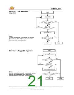
Flowchart 6 shows the toggle bit algorithm, and the section “DQ2: Toggle Bit” explains the algorithm.
See also the “DQ6: Toggle Bit I” subsection. Refer to the Toggle Bit Timings figure for the toggle bit
timing diagram. The DQ2 vs. DQ6 figure shows the differences between DQ2 and DQ6 in graphical
form.
Reading Toggle Bits DQ6/DQ2
Refer to Flowchart 6 for the following discussion. Whenever the system initially begins reading
toggle bit status, it must read DQ7–DQ0 at least twice in a row to determine whether a toggle bit is
toggling. Typically, a system would note and store the value of the toggle bit after the first read. After
the second read, the system would compare the new value of the toggle bit with the first. If the
toggle bit is not toggling, the device has completed the program or erase operation. The system can
read array data on DQ7–DQ0 on the following read cycle.
However, if after the initial two read cycles, the system determines that the toggle bit is still toggling,
the system also should note whether the value of DQ5 is high (see the section on DQ5). If it is, the
system should then determine again whether the toggle bit is toggling, since the toggle bit may have
stopped toggling just as DQ5 went high. If the toggle bit is no longer toggling, the device has
successfully completed the program or erase operation. If it is still toggling, the device did not
complete the operation successfully, and the system must write the reset command to return to
reading array data.
The remaining scenario is that the system initially determines that the toggle bit is toggling and DQ5
has not gone high. The system may continue to monitor the toggle bit and DQ5 through successive
read cycles, determining the status as described in the previous paragraph. Alternatively, it may
choose to perform other system tasks. In this case, the system must start at the beginning of the
algorithm when it returns to determine the status of the operation (top of Flowchart 6).
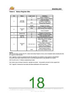
Write Operation Status
DQ7
(note2)
DQ5
(note1)
DQ2
(note2)
Operation
DQ6
DQ3
RY/BY#
Embedded Program
Algorithm
No
toggle
DQ7#
Toggle
Toggle
0
0
0
N/A
1
0
0
1
Standar
d Mode
Embedded Erase Algorithm
0
1
Toggle
Reading within Erase
Suspended Sector
Reading within Non-Erase
Suspended Sector
No
Toggle
N/A
Toggle
Erase
Suspend
Mode
Data
Data
Data
0
Data
N/A
Data
N/A
1
0
Erase-Suspend Program
DQ7#
Toggle
1. DQ5 switches to ‘1’ when an Embedded Program or Embedded Erase operation has exceeded the maximum timing limits.
See “DQ5:Exceeded Timing Limits” for more information.
2. DQ7 and DQ2 require a valid address when reading status information. Refer to the appropriate subsection for further
details.
This Data Sheet may be revised by subsequent versions
or modifications due to changes in technical specifications.
©2004 Eon Silicon Solution, Inc., www.essi.com.tw
17
Rev. D, Issue Date: 2006/11/06

 EON [ EON SILICON SOLUTION INC. ]