Preliminary EN29GL064
USER MODE DEFINITIONS
Word / Byte Configuration
The BYTE# pin controls whether the device data I/O pins operate in the byte or word configuration. If the
BYTE# pin is set at logic ‘1’, the device is in word configuration, DQ0-DQ15 are active and controlled by
CE# and OE#.
If the BYTE# pin is set at logic ‘0’, the device is in byte configuration, and only data I/O pins DQ0-DQ7
are active and controlled by CE# and OE#. The data I/O pins DQ8-DQ14 are tri-stated, and the DQ15
pin is used as an input for the LSB (A-1) address function.
VIO Control
The VIO allows the host system to set the voltage levels that the device generates and tolerates on all
inputs and outputs (address, control, and DQ signals). VIO range is 1.65 to VCC. For example, a VIO of
1.65-3.6 volts allows for I/O at the 1.65 or 3.6 volt levels, driving and receiving signals to and from other
1.65 or 3.6 V devices on the same data bus. Only 48-pin TSOP package does not offer VIO function.
Read
All memories require access time to output array data. In a read operation, data is read from one
memory location at a time. Addresses are presented to the device in random order, and the propagation
delay through the device causes the data on its outputs to arrive with the address on its inputs.
The device defaults to reading array data after device power-up or hardware reset. To read data from
the memory array, the system must first assert a valid address on A21-A0, while driving OE# and CE#
to VIL. WE# must remain at VIH. All addresses are latched on the falling edge of CE#. Data will appear
on DQ15-DQ0 after address access time (tACC), which is equal to the delay from stable addresses to
valid output data.The OE# signal must be driven to VIL. Data is output on DQ15-DQ0 pins after the
access time (tOE) has elapsed from the falling edge of OE#, assuming the tACC access time has been
meet.
Page Read Mode
The device is capable of fast page mode read and is compatible with the page mode Mask ROM read
operation. This mode provides faster read access speed for random locations within a page. The page
size of the device is 8 words/16 bytes. The appropriate page is selected by the higher address bits A21-
A3. Address bits A2-A0 in word mode (A2 to A-1 in byte mode) determine the specific word within a
page. The microprocessor supplies the specific word location.
The random or initial page access is equal to tACC or tCE and subsequent page read accesses (as long
as the locations specified by the microprocessor falls within that page) is equivalent to tPACC. When
CE# is deasserted and reasserted for a subsequent access, the access time is tACC or tCE. Fast page
mode accesses are obtained by keeping the “read-page addresses” constant and changing the “intra-
read page” addresses.
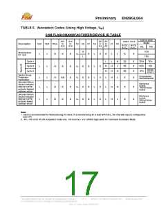
Autoselect
The Autoselect mode provides manufacturer ID, Device identification, and sector protection information,
through identifier codes output from the internal register (separate from the memory array) on DQ7-DQ0.
This mode is primarily intended for programming equipment to automatically match a device to be
programmed with its corresponding programming algorithm. The Autoselect codes can also be
accessed in-system.
There are two methods to access autoselect codes. One uses the autoselect command, the other
applies VID on address pin A9.
When using programming equipment, the autoselect mode requires VID (8.5 V to 9.5 V) on address pin
This Data Sheet may be revised by subsequent versions
or modifications due to changes in technical specifications.
©2004 Eon Silicon Solution, Inc., www.eonssi.com
18
Rev. A, Issue Date: 2009/3/20

 EON [ EON SILICON SOLUTION INC. ]