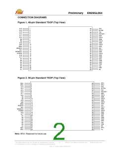
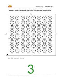
Preliminary EN29GL064
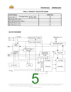
Table 2. PRODUCT SELECTOR GUIDE
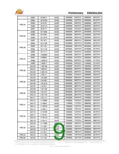
Product Number
EN29GL064
-70
Full Voltage Range: Vcc=2.7 – 3.6 V
VIO=1.65 – 3.6 V
Speed Option
Max Access Time, ns (tacc
)
70
25
70
30
Max Page Read Access, ns(tpacc
Max CE# Access, ns (tce)
Max OE# Access, ns (toe)
)
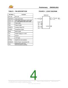
BLOCK DIAGRAM
RY/BY#
Vcc
Vss
VIO
DQ0-DQ15 (A-1)
Block Protect Switches
Erase Voltage Generator
Input/Output Buffers
State
Control
WE#
Program Voltage
Generator
Command
Register
STB
Chip Enable
Data Latch
Output Enable
Logic
CE#
OE#
Y-Decoder
Y-Gating
STB
Vcc Detector
Timer
X-Decoder
Cell Matrix
A0-AMax
This Data Sheet may be revised by subsequent versions
or modifications due to changes in technical specifications.
©2004 Eon Silicon Solution, Inc., www.eonssi.com
5
Rev. A, Issue Date: 2009/3/20

 EON [ EON SILICON SOLUTION INC. ]