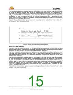
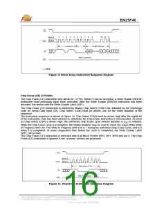
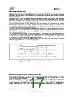
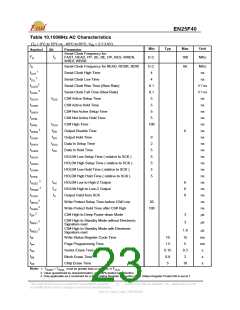
EN25F40
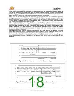
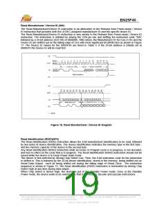
Read Manufacturer / Device ID (90h)
The Read Manufacturer/Device ID instruction is an alternative to the Release from Power-down / Device
ID instruction that provides both the JEDEC assigned manufacturer ID and the specific device ID.
The Read Manufacturer/Device ID instruction is very similar to the Release from Power-down / Device ID
instruction. The instruction is initiated by driving the CS# pin low and shifting the instruction code “90h”
followed by a 24-bit address (A23-A0) of 000000h. After which, the Manufacturer ID for Eon (1Ch) and the
Device ID are shifted out on the falling edge of CLK with most significant bit (MSB) first as shown in Figure
17. The Device ID values for the EN25F40 are listed in Table 5. If the 24-bit address is initially set to
000001h the Device ID will be read first
Figure 18. Read Manufacturer / Device ID Diagram
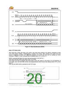
Read Identification (RDID)(9Fh)
The Read Identification (RDID) instruction allows the 8-bit manufacturer identification to be read, followed
by two bytes of device identification. The device identification indicates the memory type in the first byte ,
and the memory capacity of the device in the second byte .
Any Read Identification (RDID) instruction while an Erase or Program cycle is in progress, is not decoded,
and has no effect on the cycle that is in progress. The Read Identification (RDID) instruction should not be
issued while the device is in Deep Power down mode.
The device is first selected by driving Chip Select Low. Then, the 8-bit instruction code for the instruction
is shifted in. This is followed by the 24-bit device identification, stored in the memory, being shifted out on
Serial Data Output , each bit being shifted out during the falling edge of Serial Clock . The instruction
sequence is shown in Figure 19. The Read Identification (RDID) instruction is terminated by driving Chip
Select High at any time during data output.
When Chip Select is driven High, the device is put in the Standby Power mode. Once in the Standby
Power mode, the device waits to be selected, so that it can receive, decode and execute instructions.
This Data Sheet may be revised by subsequent versions
or modifications due to changes in technical specifications.
©2004 Eon Silicon Solution, Inc., www.essi.com.tw
19
Rev. B, Issue Date: 2007/05/09

 EON [ EON SILICON SOLUTION INC. ]