EN5339QI
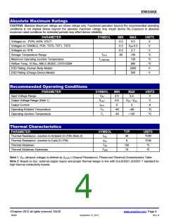
Absolute Maximum Ratings
CAUTION: Absolute Maximum ratings are stress ratings only. Functional operation beyond the recommended operating
conditions is not implied. Stress beyond the absolute maximum ratings may impair device life. Exposure to absolute
maximum rated conditions for extended periods may affect device reliability.
PARAMETER
SYMBOL
MIN
MAX
UNITS
Voltages on : PVIN, AVIN, VOUT
-0.3
6.5
V
Voltages on: ENABLE, POK, TST0, TST1, TST2
Voltages on: VFB
-0.3
-0.3
-65
VIN+0.3
2.7
V
V
Storage Temperature Range
TSTG
150
°C
°C
°C
V
Maximum Operating Junction Temperature
Reflow Temp, 10 Sec, MSL3 JEDEC J-STD-020A
ESD Rating (Human Body Model)
ESD Rating (Charge Device Model)
TJ-ABS Max
150
260
2000
500
V
Recommended Operating Conditions
PARAMETER
SYMBOL
VIN
MIN
MAX
5.5
UNITS
Input Voltage Range
2.4
0.6
0
V
V
Output Voltage Range (Note 1)
VOUT
VIN – VDO
Output Current
IOUT
TA
3
A
Operating Ambient Temperature
Operating Junction Temperature
-40
-40
+85
+125
°C
°C
TJ
Thermal Characteristics
PARAMETER
SYMBOL
TYP
UNITS
Thermal Resistance: Junction to Ambient (0 LFM) (Note 2)
36
°C/W
θJA
Thermal Resistance: Junction to Case (0 LFM)
Thermal Shutdown
6
°C/W
°C
θJC
TSD
150
15
Thermal Shutdown Hysteresis
TSDH
°C
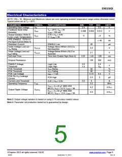
Note 1: VDO (dropout voltage) is defined as (ILOAD x Dropout Resistance). Please see Electrical Characteristics Table.
Note 2: Based on 2oz. external copper layers and proper thermal design in line with EIJ/JEDEC JESD51-7 standard for
high thermal conductivity boards.
Enpirion 2012 all rights reserved, E&OE
www.enpirion.com, Page 4
06903
September 12, 2012
Rev: B

 ENPIRION [ ENPIRION, INC. ]