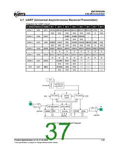
EM78P809N
8-Bit Microcontroller
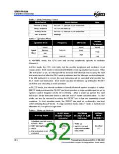
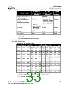
SLEEP Mode
IDLE Mode
NORMAL
Mode
Wake-up Signal
R5 (SIS) = 1+SLEP
Instruction
R5 (SIS)= 0 + SLEP
Instruction
R5 (SIS)=(*)
1. Wake-up
1. Individual interrupt source
in IMR1, IMR2
2. Jump to an Interrupt
vector after RETI
No effect
(**)
2. WDT interrupt request
3. /INT0
Interrupt
instruction, then jump
to the next instruction
or enter IDLE mode
4. Execute ENI instruction
1. Wake-up
2. Jump to the next
instruction or
enter SLEEP
mode
/SLEEP pin
No effect
No effect
/RESET pin
Reset
Reset
Reset
Reset
Reset
Reset
WDT time out
*→ Don’t care
** → Interrupt request flag will be recorded
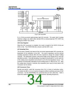
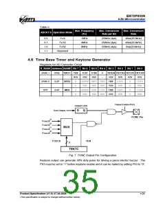
4.5 AD Converter
Registers for AD Converter Circuit
R_BANK Address NAME Bit 7 Bit 6 Bit 5 Bit 4 Bit 3 Bit 2 Bit 1 Bit 0
BANK 1
BANK 1
BANK 1
0X0B
0X0C
0X0D
ADCR ADREF ADRUN ADCK1 ADCK0 ADP
R/W R/W R/W R/W R/W
ADE7 ADE6 ADE5 ADE4 ADE3 ADE2 ADE1 ADE0
R/W R/W R/W R/W R/W R/W R/W R/W
ADD9 ADD8 ADD7 ADD6 ADD5 ADD4 ADD3 ADD2
ADIS2 ADIS1 ADIS0
R/W R/W R/W
ADIC
ADDH
R
R
R
0
R
R
R
R
R
TC2CK TC2CK TC2CK
BANK 1
0X08
ADDL
ISFR1
ADD1 ADD0
TC2M TC2S
2
1
0
R/W
TCIF3
R/W
0
R
R
--
R/W
0
R/W
R/W
R/W
SPIF
R/W
0
BANK 0
SPR
0x0E
0x0C
0x0E
EXIF5 TCIF2
R/W R/W
ADIF
R/W
EXIF3 TCIF4
0
R/W
R/W
0
ADOSCR CALI
SIGN VOF[2] VOF[1] VOF[0]
R/W
R/W
R/W
ADIE
R/W
R/W
0
R/W
--
--
--
SPR
IMR1
EXIE5 TCIE2
R/W R/W
EXIE3 TCIE4
R/W R/W
SPIE
R/W
TCIE3
R/W
0
* R_BANK : Register Bank (bits 7, 6 of R3), R/W: Read / Write
* SPR : Special Purpose Registers
Product Specification (V1.0) 07.26.2005
• 29
(This specification is subject to change without further notice)

 ELAN [ ELAN MICROELECTRONICS CORP ]