EM78P258N
8-Bit Microprocessor with OTP ROM
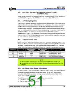
3. ADWE bit of RE register is set to “1.” Wake-up from ADC conversion (where it
remains in operation during sleep mode)
4. Wake-up and executes the next instruction if ADIE bit of IOCE0 is enabled and the
“DISI” instruction is executed
5. Wake-up and enters into Interrupt vector (address 0x00C) if ADIE bit of IOCE0 is
enabled and the “ENI” instruction is executed
6. Enters into Interrupt vector (address 0x00C) if ADIE bit of IOCE0 is enabled and the
“ENI” instruction is executed.
The results are fed into the ADDATA, ADDATA1H, and ADDATA1L registers when the
conversion is completed. If the ADIE is enabled, the device will wake up. Otherwise,
the AD conversion will be shut off, no matter what the status of ADPD bit is.
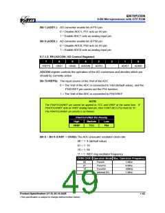
6.7.6 Programming Process/Considerations
6.7.6.1 Programming Process
Follow these steps to obtain data from the ADC:
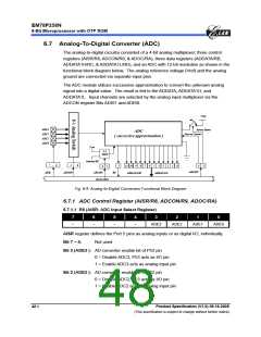
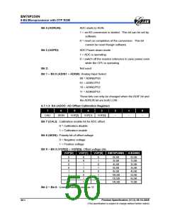
1. Write to the four bits (ADE3:ADE0) on the R8 (AISR) register to define the
characteristics of R5 (digital I/O, analog channels, or voltage reference pin)
2. Write to the R9/ADCON register to configure AD module:
a) Select ADC input channel (ADIS1:ADIS0)
b) Define AD conversion clock rate (CKR1:CKR0)
c) Select the VREFS input source of the ADC
d) Set the ADPD bit to 1 to begin sampling
3. Set the ADWE bit, if the wake-up function is employed
4. Set the ADIE bit, if the interrupt function is employed
5. Write “ENI” instruction, if the interrupt function is employed
6. Set the ADRUN bit to 1
7. Write “SLEP” instruction or Polling.
8. Wait for wake-up, ADRUN bit is cleared (“0” value), interrupt flag (ADIF) to be set
“1,” or the ADC interrupt to occurs
9. Read the ADDATA or ADDATA1H and ADDATA1L conversion data registers. If
ADC input channel changes at this time, the ADDATA, ADDATA1H, and
ADDATA1L values can be cleared to ‘0’
10. Clear the interrupt flag bit (ADIF)
11. For next conversion, go to Step 1 or Step 2 as required. At least 2 Tct is required
before the next acquisition starts.
46 •
Product Specification (V1.0) 06.16.2005
(This specification is subject to change without further notice)

 ELAN [ ELAN MICROELECTRONICS CORP ]