EM78P258N
8-Bit Microprocessor with OTP ROM
6.7.2 ADC Data Register (ADDATA/RB, ADDATA1H/RC,
ADDATA1L/RD)
When the AD conversion is completed, the result is loaded to the ADDATA, ADDATA1H
and ADDATA1L registers. The ADRUN bit is cleared, and the ADIF is set.
6.7.3 ADC Sampling Time
The accuracy, linearity, and speed of the successive approximation of AD converter are
dependent on the properties of the ADC and the comparator. The source impedance
and the internal sampling impedance directly affect the time required to charge the
sample holding capacitor. The application program controls the length of the sample
time to meet the specified accuracy. Generally speaking, the program should wait for
2µs for each KΩ of the analog source impedance and at least 2µs for the
low-impedance source. The maximum recommended impedance for analog source is
10KΩ at Vdd=5V. After the analog input channel is selected, this acquisition time must
be done before the conversion is started.
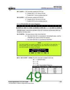
6.7.4 AD Conversion Time
CKR0 and CKR1 select the conversion time (Tct), in terms of instruction cycles. This
allows the MCU to run at the maximum frequency without sacrificing the AD conversion
accuracy. For the EM78P258N, the conversion time per bit is about 4µs. The table
below shows the relationship between Tct and the maximum operating frequencies.
Max. Operation
Frequency
Max. Conversion
Rate/Bit
CKR0:CKR1 Operation Mode
Max. Conversion Rate
00
01
10
11
Fsco/4
1 MHz
4MHz
16MHz
–
250kHz (4us)
250kHz (4us)
250kHz( 4us)
14Kkz (71us)
15*4us=60us(16.7kHz)
15*4us=60us(16.7kHz)
15*4us=60us(16.7kHz)
15*71us=1065us(0.938kHz)
Fsco/16
Fsco/64
Internal RC
NOTE
■ Pin not used as an analog input pin can be used as regular input or output pin.
■ During conversion, do not perform output instruction to maintain precision for all of
the pins.
6.7.5 ADC Operation during Sleep Mode
In order to obtain a more accurate ADC value and reduce power consumption, the AD
conversion remains operational during sleep mode. As the SLEP instruction is
executed, all the MCU operations will stop except for the Oscillator, TCC, TCCA,
TCCB, TCCC and AD conversion.
The AD Conversion is considered completed as determined by:
1. ADRUN bit of R9 register is cleared (“0” value)
2. ADIF bit of RE register is set to “1”
Product Specification (V1.0) 06.16.2005
• 45
(This specification is subject to change without further notice)

 ELAN [ ELAN MICROELECTRONICS CORP ]