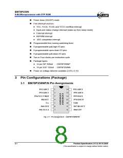
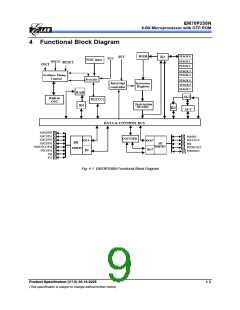
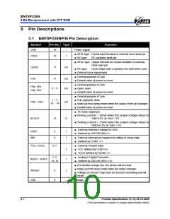
EM78P258N
8-Bit Microprocessor with OTP ROM
ꢀ
ꢀ
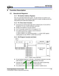
"JMP" instruction allows direct loading of the lower 10 program counter bits. Thus,
"JMP" allows PC to jump to any location within a page.
"CALL" instruction loads the lower 10 bits of the PC, and then PC+1 is pushed into
the stack. Thus, the subroutine entry address can be located anywhere within a
page.
ꢀ
ꢀ
ꢀ
ꢀ
"RET" ("RETL k", "RETI") instruction loads the program counter with the contents
of the top of stack.
"ADD R2, A" allows a relative address to be added to the current PC, and the ninth
and above bits of the PC will increase progressively.
"MOV R2, A" allows loading of an address from the "A" register to the lower 8 bits of
the PC, and the ninth and tenth bits (A8 ~ A9) of the PC will remain unchanged.
Any instruction (except “ADD R2,A”) that is written to R2 (e.g., "MOV R2, A", "BC
R2, 6",⋅⋅⋅⋅⋅) will cause the ninth bit and the tenth bit (A8 ~ A9) of the PC to remain
unchanged.
ꢀ
ꢀ
In the case of EM78P258N, the most significant bit (A10) will be loaded with the
content of PS0 in the status register (R3) upon execution of a "JMP", "CALL", or
any other instructions set which write to R2.
All instructions are single instruction cycle (fclk/2 or fclk/4) except for the
instructions that are written to R2. Note that these instructions need one or two
instructions cycle as determined by Code Option Register CYES bit.
6 •
Product Specification (V1.0) 06.16.2005
(This specification is subject to change without further notice)

 ELAN [ ELAN MICROELECTRONICS CORP ]