EM78P258N
8-Bit Microprocessor with OTP ROM
6 Function Description
6.1 Operational Registers
6.1.1 R0 (Indirect Address Register)
R0 is not a physically implemented register. Its major function is to perform as an
indirect address pointer. Any instruction using R0 as a pointer, actually accesses the
data pointed by the RAM Select Register (R4).
6.1.2 R1 (Time Clock /Counter)
ꢀ
Increased by an external signal edge which is defined by the TE bit (CONT-4)
through the TCC pin, or by the instruction cycle clock.
ꢀ
ꢀ
ꢀ
Writable and readable as any other registers
The TCC prescaler counter (IOCC1) is assigned to TCC
The contents of the IOCC1 register is cleared whenever –
• a value is written to TCC register.
• a value is written to TCC prescaler bits (Bit3, 2, 1, 0 of the CONT register)
• during power on reset, /RESET, or WDT time out reset.
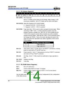
6.1.3 R2 (Program Counter) and Stack
R3
000H
003H
~
Reset Vector
A10
A9 A8
A7
~
A0
Hardware Interrupt Vector
CALL
RET
01EH
RETL
RETI
00 PAGE0 0000~03FF
01 PAGE1 0400~07FF
Stack Level 1
Stack Level 2
Stack Level 3
Stack Level 4
Stack Level 5
Stack Level 6
Stack Level 7
Stack Level 8
On-chip Program
Memory
3FEH
7FFH
Fig. 6-1 Program Counter Organization
ꢀ
ꢀ
ꢀ
R2 and hardware stacks are 12-bit wide. The structure is depicted in the table
under Section 6.1.3.1, Data Memory Configuration (next page).
Generates 2K×13 bits on-chip ROM addresses to the relative programming
instruction codes. One program page is 1024 words long.
The contents of R2 are all set to "0"s when a RESET condition occurs.
Product Specification (V1.0) 06.16.2005
• 5
(This specification is subject to change without further notice)

 ELAN [ ELAN MICROELECTRONICS CORP ]