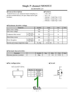
Single P-channel MOSFET
ELM33415CA-S
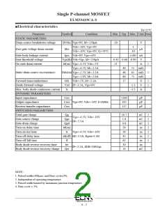
■Electrical characteristics
Ta=25°C
Parameter
Symbol
Condition
Min. Typ. Max. Unit Note
STATIC PARAMETERS
Drain-source breakdown voltage
BVdss Vgs=0V, Id=-250μA
-20
V
Vds=-16V, Vgs=0V
Idss
-1
Zero gate voltage drain current
μA
Vds=-10V, Vgs=0V, Tj=70°C
-10
Gate-body leakage current
Gate threshold voltage
On state drain current
Igss Vds=0V, Vgs=±8V
Vgs(th) Vds=Vgs, Id=-250μA
Id(on) Vgs=-4.5V, Vds=-5V
Vgs=-4.5V, Id=-3.5A
±100 nA
-0.45 -0.60 -0.90
-21
V
A
1
1
40
48
60
17
51 mΩ
61 mΩ
71 mΩ
S
Static drain-source on-resistance
Rds(on) Vgs=-2.5V, Id=-3.5A
Vgs=-1.8V, Id=-2.0A
Forward transconductance
Diode forward voltage
Max. body-diode continuous current
DYNAMIC PARAMETERS
Input capacitance
Gfs Vds=-5V, Id=-3.5A
Vsd If=-3.5A, Vgs=0V
Is
1
1
-1.3
-3.5
V
A
Ciss
1180
185
117
pF
pF
pF
Output capacitance
Coss Vgs=0V, Vds=-10V, f=1MHz
Crss
Reverse transfer capacitance
SWITCHING PARAMETERS
Total gate charge
Qg
16.7
1.8
4.6
20
nC
nC
nC
ns
2
2
2
2
2
2
2
Vgs=-4.5V, Vds=-10V
Gate-source charge
Qgs
Id=-3.5A
Qgd
Gate-drain charge
Turn-on delay time
td(on)
Turn-on rise time
tr
Vgs=-4.5V, Vds=-10V
36
ns
Turn-off delay time
td(off) Id≈-3.5A, Rgen=3.3Ω
tf
45
ns
Turn-off fall time
62
ns
Body diode reverse recovery time
Body diode reverse recovery charge
trr
30
ns
If=-3.5A, dl/dt=100A/μs
Qrr
14
nC
NOTE :
1. Pulsed width≤300μsec and Duty cycle≤2%.
2. Independent of operating temperature.
3. Pulsed width limited by maximum junction temperature.
4. Duty cycle ≤ 1%.
4 - 2

 ELM-TECH [ ELM Technology Corporation ]