EL4583C
Sync Separator, 50% Slice, S-H, Filter, H
OUT
Description of Operation
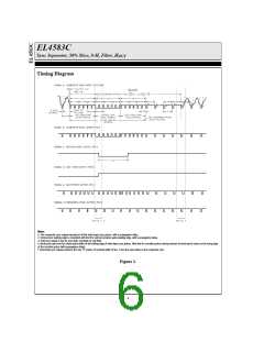
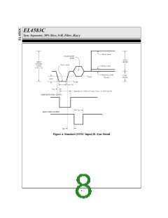
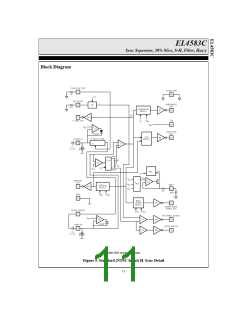
A simplified block schematic is shown in Figure 1. The
following description is intended to provide the user
with sufficient information to understand the effects of
the external components and signal conditions on the
outputs of the integrated circuit.
chip. Reference VR4 with op-amp A2 forces pin 12 to a
reference voltage of 1.7V nominal. Consequently, it can
be seen that the external resistance RSET will determine
the value of the reference current ITR. The internal resis-
tance R3 is only about 6kW, much less than RSET. All
the internal timing functions on the chip are referenced
to ITR and have excellent supply voltage rejection.
The video signal is AC coupled to pin 4 via the capacitor
C1, nominally 0.1µF. The clamp circuit A1 will prevent
the input signal on pin 4 going more negative than 1.5V,
the value of reference voltage VR1. Thus the sync tip, the
most negative part of the video waveform, will be
clamped at 1.5V. The current source I1, nominally 6µA,
charges the coupling capacitor during the remaining por-
tion of the H line, approximately 58µs for a 15.75kHz
timebase. From I • t = C • V, the video time-constant can
be calculated. It is important to note that the charge
taken from the capacitor during video must be replaced
during the sync tip time, which is much shorter, (ratio of
x 12.5). The corresponding current to restore the charge
during sync will therefore be an order of magnitude
higher, and any resistance in series with CI will cause
sync tip crushing. For this reason, the internal series
resistance has been minimized and external high resis-
tance values in series with the input coupling capacitor
should be avoided. The user can exercise some control
over the value of the input time constant by introducing
an external pull-up resistance from pin 4 to the 5V sup-
ply. The maximum voltage across the resistance will be
VDD less 1.5V, for black level. For a net discharge cur-
rent greater than zero, the resistance should be greater
than 450k. This will have the effect of increasing the
time constant and reducing the degree of picture tilt. The
current source I1 directly tracks reference current ITR
and thus increases with scan rate adjustment, as
explained later.
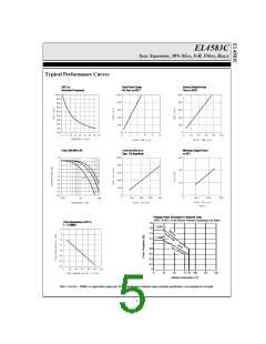
To improve noise immunity, the output of the 3 pole fil-
ter is brought out to pin 7. It is recommended to AC
couple the output to pin 8, the video input pin. In case of
strong clean video signal, the video input pin, pin 8, can
be driven by the signal directly.
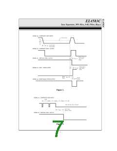
Comparator C2 on the input to the sample and hold
block (S/H) compares the leading and trailing edges of
the sync. pulse with a threshold voltage VR2 which is
referenced at a fixed level above the clamp voltage VR1
.
The output of C2 initiates the timing one-shots for gating
the sample and hold circuits. The sample of the sync tip
is delayed by 0.8µs to enable the actual sample of 2µs to
be taken on the optimum section of the sync. pulse tip.
The acquisition time of the circuit is about three horizon-
tal lines. The double poly CMOS technology enables
long time constants to be achieved with small high qual-
ity on-chip capacitors. The back porch voltage is
similarly derived from the trailing edge of sync, which
also serves to cut off the tip sample if the gate time
exceeds the tip period. Note that the sample and hold
gating times will track RSET through IOT
.
The 50% level of the sync tip is derived through the
resistor divider R1 and R2, from the sample and held
voltages VTIP and VBP and applied to the plus input of
comparator C1. This comparator has built in hysteresis
to avoid false triggering. The output of C2 is a digital 5V
signal which feeds the C/S output buffer B1, the vertical,
back porch and odd/even functions.
The signal is processed through an active 3 pole filter
(F1) designed for minimum ripple with constant phase
delay. The filter attenuates the color burst by 12dB and
eliminates fast transient spikes without sync crushing.
An external filter is not necessary. The filter also ampli-
fies the video signal by 6dB to improve the detection
accuracy. The filter cut-off frequency is controlled by an
external resistor from pin 1 to ground.
The vertical circuit senses C/S edges and initiates an
integrator which is reset by the shorter horizontal sync
pulses but times out with the longer vertical sync. pulse
widths. The internal timing circuits are referenced to IOT
and VR3, the timout period being inversely proportional
to the timing current. The vertical output pulse is started
on the first serration pulse in the vertical interval and is
Internal reference voltages (block VREF) with high
immunity to supply voltage variation are derived on the
9

 ELANTEC [ ELANTEC SEMICONDUCTOR ]