EL2070C
200MHz Current Feedback Amplifier
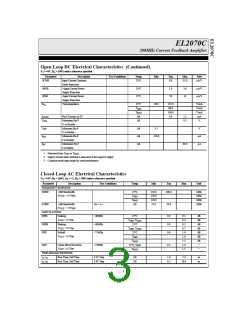
Open Loop DC Electrical Characteristics (Continued)
VS = ±5V, RL = 100W unless otherwise specified
Parameter Description
-ICMR Input Current Common
Test Conditions
Temp
Min
Typ
Max
Unit
25°C
8.0
33.0
µA/V
Mode Rejection
+IPSR
-IPSR
ROL
+Input Current Power
Supply Rejection
-Input Current Power
Supply Rejection
Transimpedance
25°C
25°C
1.0
20
3.6
24
µA/V
µA/V
25°C
TMIN
TMAX
All
30.0
125.0
80.0
140.0
0.8
V/mA
V/mA
V/mA
mA
ILOGIC
VDIS
Pin 8 Current @ 0V
Maximum Pin 8
V to Disable
1.2
0.5
All
V
VEN
IDIS
IEN
Minimum Pin 8
V to Enable
All
All
All
3.5
V
Minimum Pin 8
I to Disable
350.0
µA
µA
Maximum Pin 8
I to Enable
60.0
1. Measured from TMIN to TMAX
.
2. Supply current when disabled is measured at the negative supply.
3. Common-mode input range for rated performance.
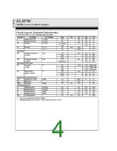
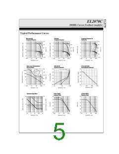
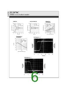
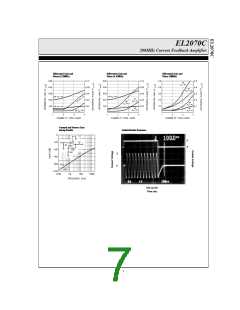
Closed-Loop AC Electrical Characteristics
VS = ±5V, RF = 250W, AV = +2, RL = 100W unless otherwise specified
Parameter
Description
Test Conditions
Temp
Min
Typ
Max
Unit
FREQUENCY RESPONSE
SSBW
LSBW
-3dB Bandwidth
25°C
TMIN
TMAX
All
150.0
150.0
120.0
35.0
200.0
50.0
MHz
MHz
MHz
MHz
(VOUT < 0.5VPP
)
-3dB Bandwidth
AV = +5
(VOUT < 5.0VPP
GAIN FLATNESS
)
GFPL
GFPH
GFR
Peaking
<40MHz
>40MHz
<75MHz
25°C
TMIN, TMAX
25°C
0.0
0.0
0.6
0.3
0.4
0.5
0.7
1.0
1.0
1.3
1.0
1.2
dB
dB
dB
dB
dB
dB
dB
°
VOUT < 0.5VPP
Peaking
VOUT < 0.5VPP
TMIN, TMAX
25°C
Rolloff
VOUT < 0.5VPP
TMIN
TMAX
LPD
Linear Phase Deviation
VOUT < 0.5VPP
<75MHz
25°C, TMIN
TMAX
0.2
°
TIME-DOMAIN RESPONSE
tr1, tf1
tr2, tf2
Rise Time, Fall Time
Rise Time, Fall Time
0.5V Step
5.0V Step
All
All
1.6
6.5
2.4
ns
ns
10.0
3

 ELANTEC [ ELANTEC SEMICONDUCTOR ]