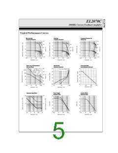
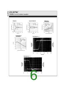
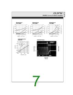
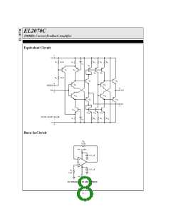
EL2070C
200MHz Current Feedback Amplifier
Absolute Maximum Ratings (T = 25°C)
A
Supply Voltage (VS)
±7V
qJA = 175°C/W SO-8
±VS
Output Current
70mA
Applied Output Voltage (Disabled)
Power Dissipation
(Output is short-circuit protected to ground, however,
See Curves
maximum reliability is obtained if I
Common-Mode Input Voltage
Differential Input Voltage
Disable Input Voltage
does not exceed 70mA)
OUT
Operating Temperature
±VS
5V
EL2070C
-40C to +85C
300°C
Lead Temperature (Soldering, 5 Seconds)
Junction Temperature
+VS, -1V
175°C
Thermal Resistance
qJA = 95°C/W P-DIP
Storage Temperature-60°C to +150°C
Important Note:
All parameters having Min/Max specifications are guaranteed. Typ values are for information purposes only. Unless otherwise noted, all tests are at the
specified temperature and are pulsed tests, therefore: TJ = TC = TA.
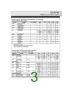
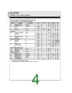
Open Loop DC Electrical Characteristics
VS = ±5V, RL = 100W unless otherwise specified
Parameter
VOS
Description
Input Offset Voltage
Test Conditions
Temp
25°C
TMIN
TMAX
All
Min
Typ
Max
5.5
Unit
mV
2
8.2
mV
9.0
mV
[1]
d(VOS)/dT
+IIN
Average Offset
Voltage Drift
+Input Current
10.0
10
40.0
µV/°C
25°C, TMAX
TMIN
25.0
36.0
µA
µA
[1]
[1]
d(+IIN)/dT
-IIN
Average +Input
Current Drift
All
50.0
10
200.0
nA/°C
-Input Current
25.0°C
TMIN, TMAX
All
30
46
µA
µA
d(-IIN)/dT
PSRR
Average -Input
Current Drift
50.0
50.0
50.0
200.0
nA/°C
Power Supply
Rejection Ratio
Common-Mode
Rejection Ratio
All
All
45.0
40.0
dB
dB
CMRR
IS
Supply Current—Quiescent
Supply Current—Disabled
+Input Resistance
No Load
[2]
All
All
16.0
4.0
20.0
7.0
mA
mA
kW
kW
pF
ISOFF
+RIN
25°C, TMAX
TMIN
100.0
50.0
200.0
CIN
Input Capacitance
All
0.5
0.1
2.0
0.2
ROUT
Output Impedance (DC)
Output Resistance (DC)
Output Capacitance (DC)
All
W
ROUT
COUT
D
D
Disabled
All
100.0
200.0
0.5
kW
pF
Disabled
[3]
All
2.0
CMIR
Common-Mode
Input Range
25°C, TMAX
TMIN
2.0
1.2
2.1
V
V
IOUT
Output Current
25°C, TMAX
TMIN
50.0
35.0
3.3
70.0
mA
mA
V
VOUT
Output Voltage Swing
Output Voltage Swing
No Load
All
3.5
3.4
VOUT
L
100W
25°C
3.0
V
2

 ELANTEC [ ELANTEC SEMICONDUCTOR ]