A Product Line of
Diodes Incorporated
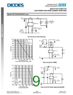
ZXCT1107/1109/1110
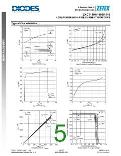
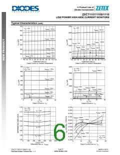
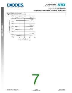
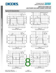
LOW POWER HIGH-SIDE CURRENT MONITORS
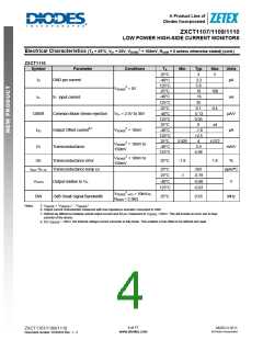
Electrical Characteristics (TA = 25°C, VS+ = 20V, VSENSE5 = 100mV, RGAIN = 0 unless otherwise stated) (cont.)
ZXCT1110
Symbol
Parameter
GND pin current
Conditions
TA
Min
Typ
3
Max
Units
25°C
-40°C
125°C
25°C
-40°C
5
IQ
µA
2.2
5.8
19
16
VSENSE5 = 0V
100
IS-
CMSR
IOO
S- input current
nA
µA/V
µA
125°C
25°C
35
0.1
0.13
0.05
0
0.4
±4
Common-Mode Sense rejection
Output Offset current6,7
Transconductance
VS+ = 2.5V to 36V
VSENSE5 = 10mV
-40°C
125°C
25°C
-40°C
125°C
25°C
-1.8
+2.5
4
3.928
4.072
VSENSE5 = 10mV to
150mV
GT
-40°C
125°C
3.9
4.08
mA/V
VSENSE5 = 10mV to
150mV
GE
Transconductance error
25°C
-1.8
-1
1.8
%
IOUT GT-TC
Transconductance temp.co
25°C
25°C
265
ppm/ºC
-0.78
-0.88
-0.63
VOUTH
BW
Output relative to VS-
-40°C
125°C
V
5
VSENSE (AC) = 10mVPP,
-3dB Small Signal Bandwidth
25°C
0.65
MHz
RGAIN = 2.5kꢀ
Notes.
5. V
= “V
” – “V
“
SENSE
SENSE+
SENSE-
6. Output current characteristic measured with low impedance ammeter connected to GND
7. Defined as difference between actual output current and 40 µA; measured at V
currents of the device.
=10mV. This will include an error due to bias
SENSE
8. For V
> 10mV, the internal voltage-current converter is fully linear. This enables a true offset to be defined and used.
SENSE
4 of 17
www.diodes.com
MARCH 2011
© Diodes Incorporated
ZXCT1107/1109/1110
Document number: DS35033 Rev. 1 - 2

 DIODES [ DIODES INCORPORATED ]