A Product Line of
Diodes Incorporated
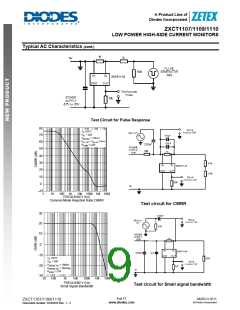
ZXCT1107/1109/1110
LOW POWER HIGH-SIDE CURRENT MONITORS
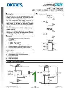
Pin Descriptions
Package
Name
OUT
SOT23
SOT23-5
ZXCT1110
3
Description
ZXCT1107
ZXCT1109
11
11
Output pin. Current output.
This is the positive input of the current monitor and has a wide
common-mode input range. This also acts as the analog supply and
provides power to internal circuitry. The current through this pin
varies with differential sense voltage.
S+
3
2
4
This is the negative input of the current monitor and has a wide
common-mode input range.
S-
2
3
5
GND
NC
-
-
-
-
2
1
Ground pin and substrate connection.
No connection
Notes.
1. For the ZXCT1107 and ZXCT1109 pin 1 (OUT) acts as both the output pin and substrate connection. This means that for the
ZXCT1107 and ZXCT1109 the minimum rail voltage that can be used is 2.5V + VOUT (see applications section for more details).
Absolute Maximum Ratings
Description
Rating
-0.3 to 40
-0.3 to 40
-0.3 to VS+
-0.3 to 0.8
±8.5
Unit
V
Voltage on S- and S+ relative to OUT (ZXCT1107/9)
Voltage on S- and S+ relative to GND (ZXCT1110)
Voltage on OUT to GND (ZXCT1110)
V
V
2,3
Differential Sense Voltage, VSENSE
V
Current into S+ and S-3
Storage Temperature
Maximum Junction Temperature
Package Power Dissipation (TA = 25°C)
SOT23
mA
°C
°C
-55 to 150
150
300 (De-rate to Zero at 150°C)
300 (De-rate to Zero at 150°C)
mW
SOT23-5
ESD Ratings
Human Body Model
Machine Model
1000
150
V
V
Operation above the absolute maximum rating may cause device failure. Operation at the absolute maximum ratings,
for extended periods, may reduce device reliability.
Notes:
2. VSENSE = V - V
S+ S-
3. The differential input voltage limit, V - V , may be exceeded provided that the input current limit into S+ or S- is not exceeded.
S+
S-
Recommended Operating Conditions
Symbol
Parameter
Min
Max
Unit
ZXCT1110
2.5
36
VS+
Common-mode input range4:
V
VOUT(MAX)
+ 2.5
ZXCT1107/9
36
VSENSE
VOUT
TA
Differential Sense Input voltage range (VS+-VS-)
Output voltage range (0 ≤ VSENSE ≤ 100mV)
Ambient temperature range
0
0
0.5
V
V
ZXCT1110
V
S- - 1
VS+ - 2.5
125
ZXCT1107/9
0
-40
°C
Notes.
4. For the ZXCT1107 and ZXCT1109 pin 1 (OUT) acts as both the output pin and substrate connection. This means that for the
ZXCT1107 and ZXCT1109 the minimum rail voltage that can be used is 2.5V + V
(see applications section for more details).
OUT
2 of 17
www.diodes.com
MARCH 2011
© Diodes Incorporated
ZXCT1107/1109/1110
Document number: DS35033 Rev. 1 - 2

 DIODES [ DIODES INCORPORATED ]