DMP2075UFDB
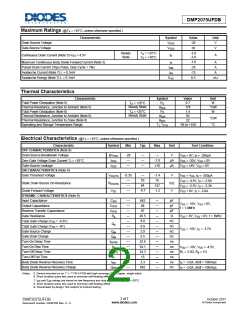
Maximum Ratings (@TA = +25°C, unless otherwise specified.)
Characteristic
Drain-Source Voltage
Symbol
VDSS
Value
-20
Unit
V
Gate-Source Voltage
±8
V
VGSS
Steady
State
-3.8
-3.0
TA = +25°C
TA = +70°C
A
Continuous Drain Current (Note 5) VGS = 4.5V
ID
-1.0
-25
-13
8.5
Maximum Continuous Body Diode Forward Current (Note 5)
Pulsed Drain Current (10µs Pulse, Duty Cycle = 1%)
Avalanche Current (Note 7) L = 0.1mH
A
A
IS
IDM
IAS
EAS
A
Avalanche Energy (Note 7) L = 0.1mH
mJ
Thermal Characteristics
Characteristic
Total Power Dissipation (Note 5)
Symbol
Value
0.7
178
Unit
W
°C/W
W
TA = +25°C
Steady State
PD
RθJA
PD
Thermal Resistance, Junction to Ambient (Note 5)
Total Power Dissipation (Note 6)
1.4
TA = +25°C
Steady State
Thermal Resistance, Junction to Ambient (Note 6)
Thermal Resistance, Junction to Case (Note 6)
Operating and Storage Temperature Range
92
RθJA
RθJC
TJ, TSTG
°C/W
°C
22
-55 to +150
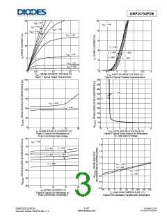
Electrical Characteristics (@TA = +25°C, unless otherwise specified.)
Characteristic
OFF CHARACTERISTICS (Note 8)
Drain-Source Breakdown Voltage
Symbol
Min
Typ
Max
Unit
Test Condition
-20
—
—
—
—
—
V
BVDSS
IDSS
VGS = 0V, ID = -250μA
VDS = -20V, VGS = 0V
VGS = ±8V, VDS = 0V
-1.0
±10
μA
μA
Zero Gate Voltage Drain Current TJ = +25°C
Gate-Source Leakage
—
IGSS
ON CHARACTERISTICS (Note 8)
Gate Threshold Voltage
-0.35
—
—
53
-1.4
75
V
mΩ
V
VGS(TH)
RDS(ON)
VSD
VDS = VGS, ID = -250μA
VGS = -4.5V, ID = -2.9A
VGS = -2.5V, ID = -2.3A
VGS = 0V, IS = -3.0A
Static Drain-Source On-Resistance
64
—
137
-1.2
-0.7
Diode Forward Voltage
—
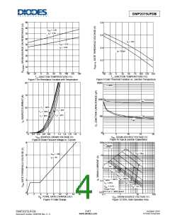
DYNAMIC CHARACTERISTICS (Note 9)
Input Capacitance
—
—
—
—
—
—
—
—
—
—
—
—
—
—
642
98
—
—
—
—
—
—
—
—
—
—
—
—
—
—
pF
pF
pF
Ω
CISS
COSS
CRSS
Rg
VDS = -10V, VGS = 0V,
f = 1.0MHz
Output Capacitance
Reverse Transfer Capacitance
Gate Resistance
87
26.5
8.8
VDS = 0V, VGS = 0V, f = 1MHz
VDS = -10V, ID = -3.7A
nC
nC
nC
nC
ns
ns
ns
ns
ns
nC
Total Gate Charge (VGS = -4.5V)
Total Gate Charge (VGS = -8V)
Gate-Source Charge
Qg
0.9
2.9
Qgs
Qgd
tD(ON)
tR
Gate-Drain Charge
5.5
Turn-On Delay Time
22.6
34.1
34.3
13
Turn-On Rise Time
VDD = -10V, VGS = -4.5V,
RL = 3.3Ω, Rg = 1Ω
Turn-Off Delay Time
tD(OFF)
tF
Turn-Off Fall Time
Body Diode Reverse Recovery Time
Body Diode Reverse Recovery Charge
3.3
tRR
IS = -3.0A, dI/dt = 100A/μs
IS = -3.0A, dI/dt = 100A/μs
642
QRR
Notes: 5. Device mounted on on 1” x 1” FR-4 PCB with high coverage 2oz. Copper, single sided.
6. Short duration pulse test used to minimize self-heating effect
7. I and E ratings are based on low frequency and duty cycles to keep T = +25°C .
AS
AS
J
8. Short duration pulse test used to minimize self-heating effect.
9. Guaranteed by design. Not subject to product testing.
2 of 7
www.diodes.com
October 2017
© Diodes Incorporated
DMP2075UFDB
Document number: DS40150 Rev. 2 - 2

 DIODES [ DIODES INCORPORATED ]