AP431/AP431A
ADJUSTABLE PRECISION SHUNT REGULATOR
Electrical Characteristics ( TA = 25oC, V+ = +5.0V, unless otherwise stated )
PARAMETER
TEST CONDITIONS
SYMBOL MIN. TYP. MAX. UNIT
VKA = VREF
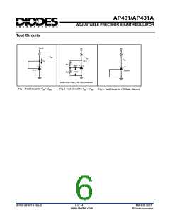
I KA = 10mA (Fig.1)
,
AP431
AP431A
2.470
2.482
2.520
2.507
Reference voltage
VREF
2.495
V
Deviation of Reference input voltage over
temperature (Note 8)
VKA = VREF, IKA = 10mA,
Ta = Full range (Fig.1)
VREF
8.0
20
mV
⎯
VKA = 10V ~VREF
VKA= 36V ~10V
R1 = 10KΩ,R2 = ∞ IKA= 10mA (Fig. 2)
R1 = 10KΩ,R2 = ∞ IKA = 10mA
Ta = Full range (Fig. 2)
∆VREF
∆VKA
IREF
-1.4
-1
1.4
-2.0
-2
3.5
mV/V
mV/V
µA
Ratio of the change in Reference voltage to
the change in Cathode voltage
⎯
⎯
⎯
IKA = 10mA (Fig. 2)
Reference input current
Deviation of Reference input current over
temperature
0.4
1.2
αIREF
⎯
µA
Minimum Cathode current for regulation
Off-state current
VKA = VREF (Fig.1)
VKA = 36V, VREF = 0V (Fig. 3)
IKA(MIN)
IKA(OFF)
0.19
0.1
0.5
1.0
mA
µA
⎯
⎯
V
KA = VREF V KA = VREF
∆IKA = 0.1mA ~ 15mA
Dynamic output impedance (Note 9)
0.2
0.5
Ω
|ZKA
|
⎯
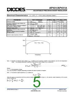
Frequency ≤ 1KHz (Fig.1)
VMAX
VMIN
VDEV = VMAX - VMIN
TI
T2
Temperature
Note: 8. Deviation of reference input voltage, VDEV, is defined as the maximum variation of the reference over the full temperature
range. The average temperature coefficient of the reference input voltage αVREF is defined as:
VDEV
(
)⋅106
VREF (25°C)
T2 − T1
ppm
……………………..……………….. (
)
α VREF
=
°C
Where:
T2 – T1 = full temperature change.
αVREF can be positive or negative depending on whether the slope is positive or negative.
Note: 9. The dynamic output impedance, RZ, is defined as:
∆VKA
∆IKA
ZKA
=
When the device is programmed with two external resistors R1 and R2 (see Figure 2.), the dynamic output impedance of the overall
circuit, is defined as:
∆v
∆i
R1
R2
'
ZKA
=
≈ZKA (1+
)
AP431/AP431A Rev. 5
5 of 14
MARCH 2007
www.diodes.com
© Diodes Incorporated

 DIODES [ DIODES INCORPORATED ]