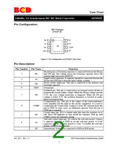
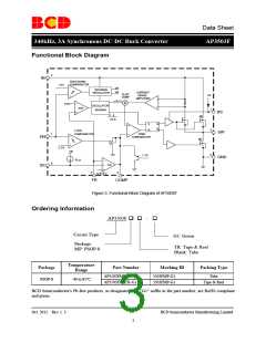
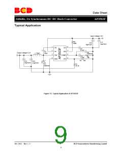
Data Sheet
340kHz, 3A Synchronous DC-DC Buck Converter
AP3503F
Absolute Maximum Ratings (Note 1)
Parameter
Symbol
VIN
Value
-0.3 to 20
-0.3 to VIN
21
Unit
V
IN Pin Voltage
EN Pin Voltage
VEN
V
SW Pin Voltage
VSW
VBS
V
BS Pin Voltage
-0.3 to VSW+6
-0.3 to 6
-0.3 to 6
-0.3 to 6
60
V
FB Pin Voltage
VFB
V
COMP Pin Voltage
SS Pin Voltage
VCOMP
VSS
V
V
Thermal Resistance
Operating Junction Temperature
Storage Temperature
Lead Temperature (Soldering, 10sec)
ESD (Human Body Model)
ESD (Machine Model)
ºC/W
ºC
ºC
ºC
V
θJA
TJ
150
TSTG
TLEAD
VHBM
VMM
-65 to 150
260
2000
200
V
Note 1: Stresses greater than those listed under “Absolute Maximum Ratings” may cause permanent damage to
the device. These are stress ratings only, and functional operation of the device at these or any other conditions
beyond those indicated under “Recommended Operating Conditions” is not implied. Exposure to “Absolute
Maximum Ratings” for extended periods may affect device reliability.
Recommended Operating Conditions
Parameter
Symbol
VIN
Min
4.5
Max
18
Unit
V
Input Voltage
Operating Ambient Temperature
TA
-40
85
ºC
Oct. 2012 Rev. 1. 3
BCD Semiconductor Manufacturing Limited
4

 DIODES [ DIODES INCORPORATED ]