Data Sheet
340kHz, 3A Synchronous DC-DC Buck Converter
AP3503F
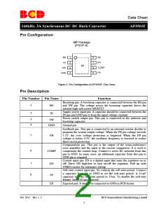
Pin Configuration
MP Package
(PSOP-8)
8
1
2
3
4
7
6
5
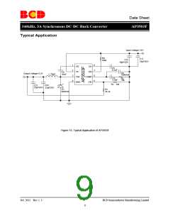
Figure 2. Pin Configuration of AP3503F (Top View)
Pin Description
Pin Number Pin Name
Function
Bootstrap pin. A bootstrap capacitor is connected between the BS pin
and SW pin. The voltage across the bootstrap capacitor drives the
internal high-side power MOSFET
Supply power input pin. A capacitor should be connected between the
IN pin and GND pin to keep the input voltage constant
Power switch output pin. This pin is connected to the inductor and
bootstrap capacitor
1
2
BS
IN
3
4
SW
GND
Ground pin
Feedback pin. This pin is connected to an external resistor divider to
program the system output voltage. When the FB pin voltage exceeds
1.1V, the over voltage protection is triggered. When the FB pin
voltage is below 0.3V, the oscillator frequency is lowered to realize
short circuit protection
Compensation pin. This pin is the output of the transconductance
error amplifier and the input to the current comparator. It is used to
compensate the control loop. Connect a series RC network from this
pin to GND. In some cases, an additional capacitor from this pin to
GND pin is required
Control input pin. EN is a digital input that turns the regulator on or
off. Drive EN high/low to turn on/off the regulator. Pull up with
100kΩ resistor for automatic startup
Soft-start control input pin. SS controls the soft-start period. Connect
a capacitor from SS to GND to set the soft-start period. A 0.1μF
capacitor sets the soft-start period to 15ms. To disable the soft-start
feature, leave SS unconnected
5
6
FB
COMP
EN
7
8
SS
EP
Exposed pad. It should be connected to GND in PCB layout
Oct. 2012 Rev. 1. 3
BCD Semiconductor Manufacturing Limited
2

 DIODES [ DIODES INCORPORATED ]