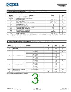
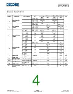
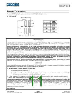
74AUP1G04
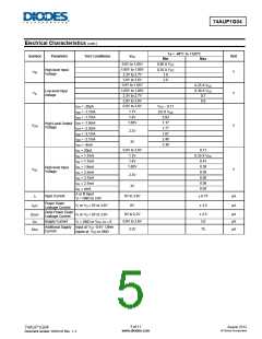
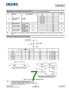
Operating and Package Characteristics (@TA = +25°C, unless otherwise specified.)
Parameter
Test Conditions
Typ
6.5
Unit
VCC
0.8V
1.2V ± 0.1V
1.5V ± 0.1V
1.8V ± 0.15V
2.5V ± 0.2V
3.3V ± 0.3V
0V or 3.3V
6.3
6.3
Power Dissipation
Capacitance
f = 1MHz
No Load
pF
Cpd
6.2
6.2
6.1
Input Capacitance
1.5
pF
Ci
Vi = VCC or GND
SOT353
371
430
445
143
190
250
Thermal Resistance
Junction-to-Ambient
X2-DFN1410-6
X2-DFN1010-6
SOT353
(Note 6)
(Note 6
°C/W
θJA
Thermal Resistance
Junction-to-Case
X2-DFN1410-6
X2-DFN1010-6
°C/W
θJC
Note:
6. Test condition for SOT353, DFN1410, and DFN1010 devices mounted on FR-4 substrate PC board, 2oz copper, with minimum recommended pad
layout.
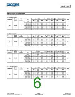
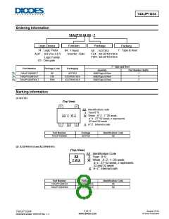
Parameter Measurement Information
Inputs
VCC
VM
CL
VI
tr/tf
0.8V
≤3ns
≤3ns
≤3ns
≤3ns
≤3ns
≤3ns
5, 10, 15, 30pF
5, 10, 15, 30pF
5, 10, 15, 30pF
5, 10, 15, 30pF
5, 10, 15, 30pF
5, 10, 15, 30pF
VCC
VCC
VCC
VCC
VCC
VCC
VCC/2
VCC/2
VCC/2
VCC/2
VCC/2
VCC/2
1.2V±0.1V
1.5V±0.1V
1.8V±0.15V
2.5V±0.2V
3.3V±0.3V
Voltage Waveform Pulse Duration
Voltage Waveform Propagation Delay Times
Inverting and Non Inverting Outputs
Figure 1. Load Circuit and Voltage Waveforms
A. Includes test lead and test apparatus capacitance.
Notes:
B. All pulses are supplied at pulse repetition rate ≤ 10 MHz.
C. Inputs are measured separately one transition per measurement.
D. tPLH and tPHL are the same as tPD.
7 of 11
www.diodes.com
August 2012
© Diodes Incorporated
74AUP1G04
Document number: DS35147 Rev. 1- 2

 DIODES [ DIODES INCORPORATED ]