DA14580
FINAL
Bluetooth Low Energy 4.2 SoC
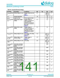
Table 257: Absolute Maximum Ratings
Parameter
Description
Conditions
Min
Typ
Max
Unit
V
t)
(defaul limiting voltage on a pin
Voltage between pin and
GND
(Note 7)
-0.1
min{3.6,
VBAT_RF
+0.2}
V
PIN(LIM)
T
storage temperature
supply rise time
-50
150
100
3.6
°C
ms
V
STG
t
Power supply rise time
R(SUP)
V
1V)
(VBAT limiting battery supply
voltage
Supply voltage on
VBAT1V in a boost con-
verter application
(VBAT3V is second out-
put of boost-converter in
this case)
-0.1
BAT(LIM)
(Note 7)
V
3V)
(VBAT limiting battery supply
voltage
Supply voltage on
VBAT3V and VBAT_RF
in a buck-converter
application, pin VBAT1V
is connected to ground
(Note 7)
-0.1
3.6
V
BAT(LIM)
V
V
(1V2)
(VDC
limiting voltage on a pin
XTAL32Km, XTAL16Mp,
XTAL16Mm
(Note 7)
-0.2
-0.2
-0.2
min(1.2,V
BAT_RF+
0.2)
V
V
V
V
V
V
PIN(LIM)
limiting voltage on the
VDCDC_RF pin
Supply voltage on
VDCDC_RF
(Note 7)
min(3.3,V
BAT_RF+
0.2)
PIN(LIM)
DC_RF)
V
(XTAL limiting voltage on a pin
XTAL32Kp
min(1.5,V
BAT_RF+
0.2)
PIN(LIM)
32Kp)
V
(WL electrostatic discharge
voltage (Human Body
Model)
2000
4000
4000
ESD(HBM)
CSP34)
V
(QF
electrostatic discharge
voltage (Human Body
Model)
ESD(HBM)
N40)
V
(QF
electrostatic discharge
voltage (Human Body
Model)
ESD(HBM)
N48)
V
(WLC electrostatic discharge
voltage (Machine Model)
200
200
200
500
V
V
V
V
ESD(MM)
SP34)
V
(QFN electrostatic discharge
voltage (Machine Model)
ESD(MM)
40)
V
(QFN electrostatic discharge
voltage (Machine Model)
ESD(MM)
48)
V
(WL electrostatic discharge
voltage (Charged Device
Model)
ESD(CDM)
CSP34)
V
N40)
(QF
electrostatic discharge
voltage (Charged Device
Model)
1000
1000
V
V
ESD(CDM)
V
(QF
electrostatic discharge
voltage (Charged Device
Model)
ESD(CDM)
N48)
Datasheet
Revision 3.4
09-Nov-2016
CFR0011-120-01
141 of 155
© 2014 Dialog Semiconductor

 DIALOG [ Dialog Semiconductor ]