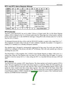
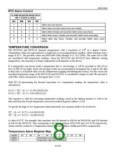
DS1921H/Z
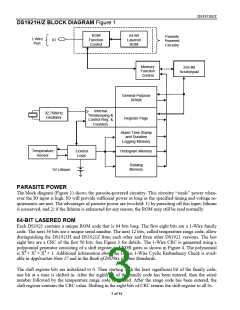
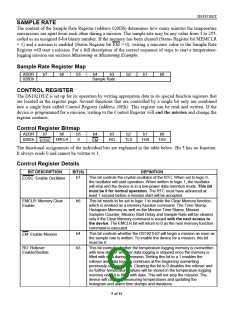
DS1921H/Z BLOCK DIAGRAM Figure 1
ROM
Function
Control
64-Bit
Lasered
ROM
Parasite
Powered
Circuitry
1-Wire
Port
IO
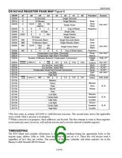
Memory
Function
Control
256-Bit
Scratchpad
General-Purpose
SRAM
Internal
32.768kHz
Oscillator
Timekeeping &
Control Reg. &
Counters
Register Page
Alarm Time Stamp
and Duration
Logging Memory
Temperature
Sensor
Control
Logic
Histogram Memory
Datalog
Memory
3V Lithium
PARASITE POWER
The block diagram (Figure 1) shows the parasite-powered circuitry. This circuitry “steals” power when-
ever the IO input is high. IO will provide sufficient power as long as the specified timing and voltage re-
quirements are met. The advantages of parasite power are two-fold: 1) by parasiting off this input, lithium
is conserved, and 2) if the lithium is exhausted for any reason, the ROM may still be read normally.
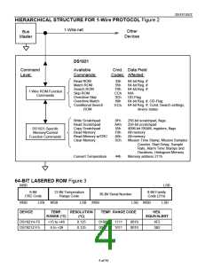
64-BIT LASERED ROM
Each DS1921 contains a unique ROM code that is 64 bits long. The first eight bits are a 1-Wire family
code. The next 36 bits are a unique serial number. The next 12 bits, called temperature range code, allow
distinguishing the DS1921H and DS1921Z from each other and from other DS1921 versions. The last
eight bits are a CRC of the first 56 bits. See Figure 3 for details. The 1-Wire CRC is generated using a
polynomial generator consisting of a shift register and XOR gates as shown in Figure 4. The polynomial
is X8 + X5 + X4 + 1. Additional information about the Dallas 1-Wire Cyclic Redundancy Check is avail-
able in Application Note 27 and in the Book of DS19xx iButton Standards.
The shift register bits are initialized to 0. Then starting with the least significant bit of the family code,
one bit at a time is shifted in. After the eighth bit of the family code has been entered, then the serial
number followed by the temperature range code is entered. After the range code has been entered, the
shift register contains the CRC value. Shifting in the eight bits of CRC returns the shift register to all 0s.
3 of 44

 DALLAS [ DALLAS SEMICONDUCTOR ]