DS1085
Table 1. DEVICE COMPARISONS BY PART NUMBER
PART NUMBER
DS1085Z-10
STEP SIZE (kHz)
DAC SPAN (MHz)
OFFSET SIZE (MHz)
10
25
50
10.24
25.60
51.20
5.12
6.40
6.40
DS1085Z-25
DS1085Z-50
For further description of use of the OFFSET register, see the REGISTER FUNCTIONS section.
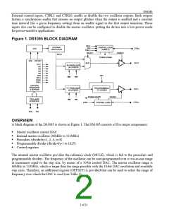
The master clock can be routed directly to the outputs (OUT0 and OUT1) or through separate prescalers
(P0 and P1). In the case of OUT1, an additional programmable divider (N) can be used to generate
frequencies down to 8.1kHz.
The prescaler (P0) divides MCLK by 1, 2, 4, or 8 before routing MCLK to the reference output (OUT0)
pin.
The prescaler (P1) divides MCLK by 1, 2, 4, or 8 before routing MCLK to the programmable divider (N),
and, ultimately, the main output (OUT1) pin.
The programmable divider (N) divides the prescaler output (P1) by any number selected between two and
1025 (10 bits) to provide the main output (OUT1), or it can be bypassed altogether by use of the DIV1
register bit. The value of N is stored in the DIV register.
The control registers are user-programmable through a 2-wire serial interface to determine operating
frequency (values of DAC, OFFSET, P0, P1, and N) and modes of operation. Once programmed, the
register settings are nonvolatile and only need reprogramming if it is desired to reconfigure the device.
PIN DESCRIPTIONS
PIN
NAME
DESCRIPTION
This main oscillator output frequency is determined by the control
register settings for the oscillator (DAC and OFFSET), prescaler P1
(mode bits 1M0 and 1M1), and divider N (DIV).
1
OUT1
The reference output is taken from the output of the reference select mux.
Its frequency is determined by the control register settings for prescaler
P0 (mode bits 0M0 and 0M1) (see Table 2).
2
OUT0
3
4
VCC
GND
Power Supply
Ground
A multifunction control input pin that can be programmed to function as
a mux select, output enable, and/or a power-down. Its function is
determined by the user-programmable control register values of EN0,
SEL0, and PDN0 (see Table 2).
5
CTRL0
A multifunction control input pin that can be programmed to function as
an output enable and/or a power-down. Its function is determined by the
user-programmable control register value of PDN1 (see Table 3).
I/O pin for the 2-wire serial interface used for data transfer.
Input pin for the 2-wire serial interface used to synchronize data
movement over the serial interface.
6
CTRL1
7
8
SDA
SCL
3 of 21

 DALLAS [ DALLAS SEMICONDUCTOR ]