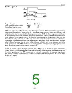
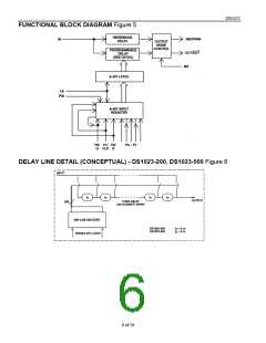
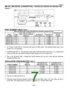
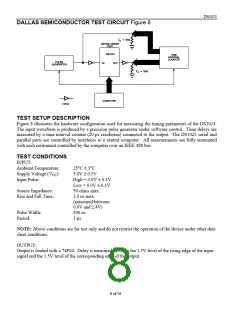
DS1023
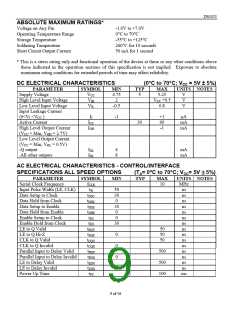
ABSOLUTE MAXIMUM RATINGS*
Voltage on Any Pin
-1.0V to +7.0V
Operating Temperature Range
Storage Temperature
Soldering Temperature
0°C to 70°C
-55°C to +125°C
260°C for 10 seconds
50 mA for 1 second
Short Circuit Output Current
* This is a stress rating only and functional operation of the device at these or any other conditions above
those indicated in the operation sections of this specification is not implied. Exposure to absolute
maximum rating conditions for extended periods of time may affect reliability.
DC ELECTRICAL CHARACTERISTICS
(0°C to 70°C; VCC = 5V ± 5%)
PARAMETER
Supply Voltage
High Level Input Voltage
Low Level Input Voltage
Input Leakage Current
SYMBOL
VCC
MIN
4.75
2
TYP
5
MAX
5.25
UNITS NOTES
V
V
V
VIH
VCC +0.5
0.8
VIL
-0.5
(0<VI <VCC
Active Current
)
II
ICC
IOH
-1
+1
60
-1
µA
mA
mA
30
High Level Output Current
(VCC = Min, VOH = 2.7V)
Low Level Output Current
(VCC = Min, VOL = 0.5V)
-Q output
IOL
IOL
4
8
mA
mA
-All other outputs
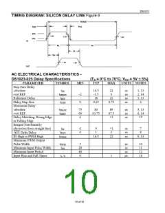
AC ELECTRICAL CHARACTERISTICS - CONTROL/INTERFACE
SPECIFICATIONS ALL SPEED OPTIONS
(TA= 0°C to 70°C; VCC= 5V ±=5%)
PARAMETER
Serial Clock Frequency
Input Pulse Width (LE, CLK)
Data Setup to Clock
Data Hold from Clock
Data Setup to Enable
Data Hold from Enable
Enable Setup to Clock
Enable Hold from Clock
LE to Q Valid
SYMBOL
fCLK
tW
MIN
TYP
MAX
UNITS NOTES
10
MHz
ns
ns
ns
ns
ns
ns
ns
ns
ns
ns
ns
ns
ns
ns
ns
ms
50
30
0
30
0
tDSC
tDHC
tDSE
tDHE
tES
0
30
tEH
tEQV
tEQZ
tCQV
tCQX
tPDV
tPDX
tEDV
tEDX
tPU
50
50
50
LE to Q Hi-Z
CLK to Q Valid
CLK to Q Invalid
Parallel Input to Delay Valid
Parallel Input to Delay Invalid
LE to Delay Valid
LE to Delay Invalid
Power Up Time
0
0
0
0
500
500
100
9 of 16

 DALLAS [ DALLAS SEMICONDUCTOR ]