DS1023
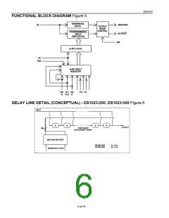
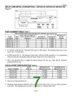
DELAY LINE DETAIL (CONCEPTUAL) - DS1023-25, DS1023-50, DS1023-100
Figure 7
PART NUMBER TABLE Table 1
DELAYS RANGES AND TOLERANCE (all times measured in ns)
MAX. DELAY TIME (1)/
MINIMUM I/P
PART
STEP MAX. OUTPUT PULSE
MAXIMUM
DEVIATION (3)
MAXIMUM
I/P FREQ
25 MHz
PULSE
WIDTH
NUMBER
DS1023-025
DS1023-050
DS1023-100
DS1023-200
DS1023-500
SIZE
0.25
0.50
1.0
WIDTH (2)
63.75
127.5
255
20
20
20
20
50
±1
±2
±4
±8
±20
25 MHz
25 MHz
25 MHz
10 MHz
2.0
510
5.0
1275
1. In “Normal” mode (MS=0). Measured with respect to REF output. The minimum delay time is zero
(or less, by 1.5 ns typically)
2. In PWM mode (MS=1). The minimum output pulse width for reliable operation is 5 ns; programmed
values less than this may produce reduced output voltage levels or no output at all.
3. This is the deviation from a straight line drawn between the step zero value and the maximum
programmed delay time.
OSCILLATOR CONFIGURATION Table 2
STEP
SIZE (4)
0.5
MINIMUM O/P
FREQUENCY (5)
6.6 MHz
MAXIMUM O/P
FREQUENCY (5)
22 MHz
PART NUMBER
DS1023-025
DS1023-050
DS1023-100
DS1023-200
DS1023-500
1.0
2.0
3.6 MHz
1.9 MHz
0.98 MHz
0.4 MHz
22 MHz
22 MHz
22 MHz
22 MHz
4.0
10.0
4. Step size in output period (in ns).
5. Maximum output frequency depends on the actual step zero delay value, worst case values are shown
in the table. The output period is given by: 2 * tD where: tD = absolute delay value.
7 of 16

 DALLAS [ DALLAS SEMICONDUCTOR ]