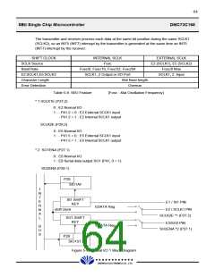
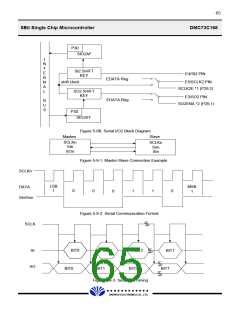
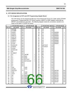
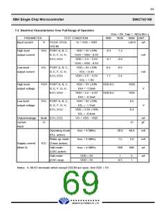
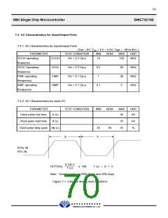
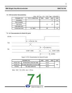
68
8Bit Single Chip Microcontroller
DMC73C168
* Stresses beyond those listed under "Absolute Maximum Ratings" may cause permanent damage
to the device. This is a stress rating only and functional operating of the device at those or any other
conditions beyond those indicated in the "Recommended Operating Conditions" section of this
specification is not implied. Exposure to absolute-maximumrated conditions for extended periods
may affect device reliability.
Notes :
1. Unless otherwise noted, all voltages are with respect to VSS.
2. Test pin must connect to VSS.
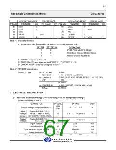
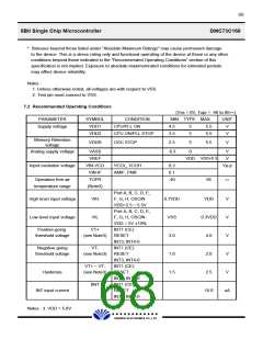
7.2 Recommended Operating Conditions
(Vss = 0V, Topr = -40 to 85¡ É)
PARAMETER
Supply voltage
SYMBOL
VDD1
CONDITION
CPU/PLL ON
MIN TYPE MAX
UNIT
V
4.5
5
5
5.5
VDD2
CPU ON/PLL STOP
OSC STOP
3.5
2.5
5.5
5.5
V
Memory Retention
voltage
VDDR
5
V
Analog supply voltage
VASS
VREF
-0.3
0
V
V
VDD+0.3
85
VDD
Input oscilation voltage
VIN-VCO
VIN-IF
VCOL, VCOH
AMIF, FMIF
0.3
0.1
-40
Vp-p
Operation free air
temperature range
TOPR
¡ É
(Note3)
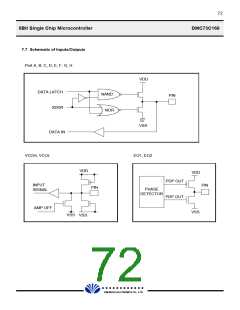
Port A, B, C, D, E,
F, G, H, OSCIN
VDD=2.5 ~ 5.5V
Port A, B, C, D, E,
F, G, H, OSCIN
VDD = 5V ±10%
INT1 (CE)
High level input voltage
Low level input voltage
VIH
VIL
0.7VDD
VSS
3.0
VDD
0.3VDD
4.0
V
V
Positive-going
VT+
threshold voltage
(see Note3)
RESET
V
INT3, INT4-0
INT1 (CE)
Negative-going
VT-
threshold voltage
(see Note3)
RESET
1.0
2.0
V
INT3, INT4-0
INT1 (CE)
VT+ ~ VT-
Hysterisis
INT input current
(see Note3)
RESET
1.5
2.5
V
INT3, INT4-0
INT1 (CE)
IINT
RESET
10.0
uA
INT3, INT4-0
Notes : 3. VDD = 5.0V
£Ä£Á£Å£×£Ï £Ï
DAEWOO ELECTRONICS CO., LTD.

 DAEWOO [ DAEWOO Electronic Components ]