Spec. No. : C855T3
Issued Date : 2004.12.15
Revised Date :
CYStech Electronics Corp.
Page No. : 4/4
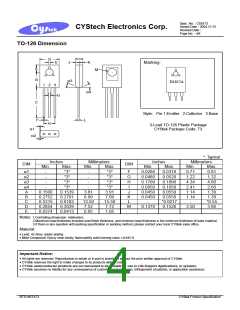
TO-126 Dimension
I
D
E
J
K
Marking:
A
B
M
α 3
D1857A
2
1
3
α 4
G
C
Style: Pin 1.Emitter 2.Collector 3.Base
F
L
H
3-Lead TO-126 Plastic Package
CYStek Package Code: T3
α1
α 2
*: Typical
Inches
Millimeters
Inches
Min.
Millimeters
DIM
DIM
Min.
Max.
*3°
Min.
-
Max.
*3°
Max.
0.0319
0.0520
0.1890
0.1050
0.0550
0.0550
*0.0217
0.1520
Min.
Max.
0.81
1.32
4.80
2.66
1.39
1.39
*0.55
3.86
-
F
G
H
I
0.0280
0.0480
0.1709
0.0950
0.0450
0.0450
-
0.71
1.22
4.34
2.41
1.14
1.14
-
α1
α2
α3
α4
A
-
-
*3°
*3°
-
-
*3°
*3°
*3°
-
-
*3°
0.1500
0.2752
0.5315
0.2854
0.0374
0.1539
0.2791
0.6102
0.3039
0.0413
3.81
6.99
13.50
7.52
0.95
3.91
7.09
15.50
7.72
1.05
J
B
K
L
C
D
M
0.1378
3.50
E
Notes: 1.Controlling dimension: millimeters.
2.Maximum lead thickness includes lead finish thickness, and minimum lead thickness is the minimum thickness of base material.
3.If there is any question with packing specification or packing method, please contact your local CYStek sales office.
Material:
• Lead: 42 Alloy; solder plating
• Mold Compound: Epoxy resin family, flammability solid burning class: UL94V-0
Important Notice:
• All rights are reserved. Reproduction in whole or in part is prohibited without the prior written approval of CYStek.
• CYStek reserves the right to make changes to its products without notice.
• CYStek semiconductor products are not warranted to be suitable for use in Life-Support Applications, or systems.
• CYStek assumes no liability for any consequence of customer product design, infringement of patents, or application assistance.
BTD1857AT3
CYStek Product Specification

 CYSTEKEC [ CYSTECH ELECTONICS CORP. ]