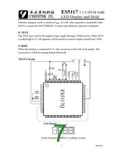
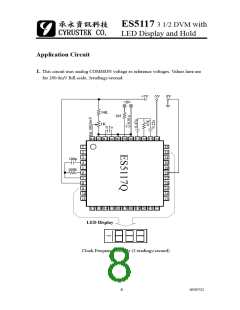
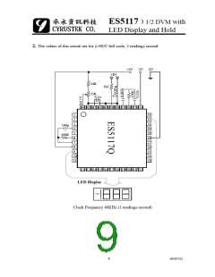
ES5117 3 1/2 DVM with
LED Display and Hold
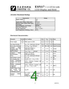
Absolute Maximum Ratings
Characteristic
Supply Voltage V+
Rating
+6V
V-
-6V
Analog Input Voltage (either input)
Reference input voltage (either input)
Clock input
Power Dissipation. Flat Package
Operating Temperature
Storage Temperature
Lead Temperature (Soldering, 10sec)
V+ to V-
V+ to V-
GND to V+
800mW
0℃ to 70℃
-65℃ to 160℃
270℃
Electrical Characteristics
Parameter
Symbol Test Condition
V+
Min.
+4
-4
Typ.
+5
-5
Max Units
+6
-6
Power Supply
With respect to GND
V
V-
-
± 000.0
Zero Input Reading
Ratio-metric Reading
-000.0
+000.0 Digital Reading
VIN = 0V , Full-Scale=200.0mV
VIN=VREF , VREF=100.0mV
-
999 999/1000 1000 Digital Reading
Linearity
(Max.
Full-Scale=200mV or
Full-Scale=2.000V
± 0.2
deviation form best
straight line fit)
-
-1
+1 Counts
+1 Counts
± 0.2
Roll-over Error
-
-
-VIN = +VIN
~
200.0mV
-1
-
VCM=± 1V, VIN=0V
Full-Scale=200.0mV
VIN = 0V , Full-Scale=200.0mV
VIN = 0V
Common
Mode
50
-
-
uV/V
Rejection Ratio
Noise
Input leakage current
Zero Reading Drift
-
-
-
-
-
-
15
1
0.2
uVp-p
10 pA
VIN=0V , 0℃ <= TA <= 70℃
uV/℃
1
Analog COMMON
Voltage ( with respect
to V+)
25K Ω Between Common and
-
-
2.8
-
3.0
60
3.2
V
Positive Supply
Analog COMMON
Temperature
25K Ω Between Common and
V+ , 0℃ <= TA <= 70℃
ppm/℃
75
Coefficient
Supply Current (Does
not include LED
drive current and
COMMON current)
-
VIN=0V
-
0.6
0.75 mA
mA
V+ = 5.0V,
Segment
Except pin26
pin26 only
5
8
Segment
Current
Sinking
10
16
Voltage=3V
4
03/07/21

 CYRUSTEK [ Cyrustek corporation ]