CY8C24x23 Final Data Sheet
PSoC™ Overview
Document Conventions
Table of Contents
For an in depth discussion and more information on your PSoC
device, obtain the PSoC Mixed Signal Array Technical Refer-
ence Manual. This document encompasses and is organized
into the following chapters and sections.
Acronyms Used
The following table lists the acronyms that are used in this doc-
ument.
1.
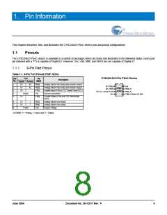
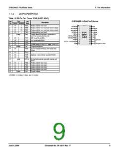
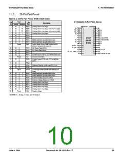
Pin Information ............................................................. 8
Acronym
AC
Description
alternating current
1.1 Pinouts ................................................................... 8
1.1.1 8-Pin Part Pinout ....................................... 8
1.1.2 20-Pin Part Pinout ..................................... 9
1.1.3 28-Pin Part Pinout ................................... 10
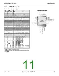
1.1.4 32-Pin Part Pinout .................................... 11
ADC
API
analog-to-digital converter
application programming interface
central processing unit
continuous time
CPU
CT
DAC
DC
digital-to-analog converter
direct current
2.
3.
Register Reference ..................................................... 12
2.1 Register Conventions ........................................... 12
2.1.1 Abbreviations Used .................................. 12
2.2 Register Mapping Tables ..................................... 12
EEPROM
FSR
GPIO
IO
electrically erasable programmable read-only memory
full scale range
general purpose IO
Electrical Specifications ............................................ 15
input/output
3.1 Absolute Maximum Ratings ................................ 16
3.2 Operating Temperature ....................................... 16
3.3 DC Electrical Characteristics ................................ 17
3.3.1 DC Chip-Level Specifications ................... 17
3.3.2 DC General Purpose IO Specifications .... 17
3.3.3 DC Operational Amplifier Specifications ... 18
3.3.4 DC Analog Output Buffer Specifications ... 20
3.3.5 DC Switch Mode Pump Specifications ..... 21
3.3.6 DC Analog Reference Specifications ....... 22
3.3.7 DC Analog PSoC Block Specifications ..... 23
3.3.8 DC POR and LVD Specifications ............. 24
3.3.9 DC Programming Specifications ............... 25
3.4 AC Electrical Characteristics ................................ 26
3.4.1 AC Chip-Level Specifications ................... 26
3.4.2 AC General Purpose IO Specifications .... 28
3.4.3 AC Operational Amplifier Specifications ... 29
3.4.4 AC Digital Block Specifications ................. 31
3.4.5 AC Analog Output Buffer Specifications ... 32
3.4.6 AC External Clock Specifications ............. 33
3.4.7 AC Programming Specifications ............... 33
3.4.8 AC I2C Specifications ............................... 34
IPOR
LSb
imprecise power on reset
least-significant bit
LVD
low voltage detect
MSb
PC
most-significant bit
program counter
POR
PPOR
PSoC™
PWM
RAM
ROM
SC
power on reset
precision power on reset
Programmable System-on-Chip
pulse width modulator
random access memory
read only memory
switched capacitor
SMP
switch mode pump
Units of Measure
A units of measure table is located in the Electrical Specifica-
tions section. Table 3-1 on page 15 lists all the abbreviations
used to measure the PSoC devices.
4.
Packaging Information ............................................... 35
4.1 Packaging Dimensions ......................................... 35
4.2 Thermal Impedances .......................................... 40
4.3 Capacitance on Crystal Pins ............................... 40
Numeric Naming
Hexidecimal numbers are represented with all letters in upper-
case with an appended lowercase ‘h’ (for example, ‘14h’ or
‘3Ah’). Hexidecimal numbers may also be represented by a ‘0x’
prefix, the C coding convention. Binary numbers have an
appended lowercase ‘b’ (e.g., 01010100b’ or ‘01000011b’).
Numbers not indicated by an ‘h’ or ‘b’ are decimal.
5.
6.
Ordering Information .................................................. 41
5.1 Ordering Code Definitions ................................... 41
Sales and Company Information ............................... 42
6.1 Revision History .................................................. 42
6.2 Copyrights ............................................................ 42
June 4, 2004
Document No. 38-12011 Rev. *F
7

 CYPRESS [ CYPRESS ]