CY7C68013A/CY7C68014A
CY7C68015A/CY7C68016A
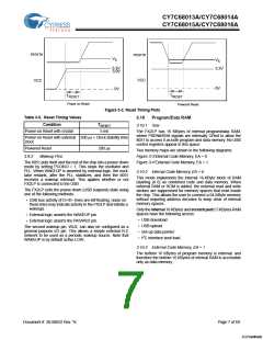
The CLKOUT pin, which can be three-stated and inverted
using internal control bits, outputs the 50% duty cycle 8051
clock, at the selected 8051 clock frequency—48, 24, or 12
MHz.
3.0
3.1
Functional Overview
USB Signaling Speed
FX2LP operates at two of the three rates defined in the USB
Specification Revision 2.0, dated April 27, 2000:
3.2.2
USARTS
• Full speed, with a signaling bit rate of 12 Mbps
• High speed, with a signaling bit rate of 480 Mbps.
FX2LP contains two standard 8051 USARTs, addressed via
Special Function Register (SFR) bits. The USART interface
pins are available on separate I/O pins, and are not multi-
plexed with port pins.
FX2LP does not support the low-speed signaling mode of
1.5 Mbps.
UART0 and UART1 can operate using an internal clock at
230 KBaud with no more than 1% baud rate error. 230-KBaud
operation is achieved by an internally derived clock source that
generates overflow pulses at the appropriate time. The
internal clock adjusts for the 8051 clock rate (48, 24, 12 MHz)
such that it always presents the correct frequency for
230-KBaud operation.[1]
3.2
8051 Microprocessor
The 8051 microprocessor embedded in the FX2LP family has
256 bytes of register RAM, an expanded interrupt system,
three timer/counters, and two USARTs.
3.2.1
8051 Clock Frequency
3.2.3
Special Function Registers
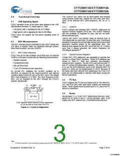
FX2LP has an on-chip oscillator circuit that uses an external
24-MHz (±100-ppm) crystal with the following characteristics:
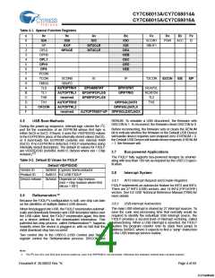
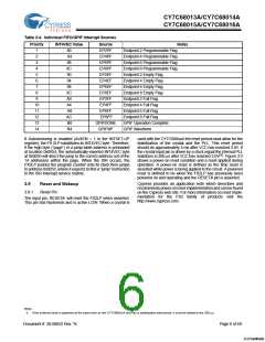
Certain 8051 SFR addresses are populated to provide fast
access to critical FX2LP functions. These SFR additions are
shown in Table 3-1. Bold type indicates non-standard,
enhanced 8051 registers. The two SFR rows that end with “0”
and “8” contain bit-addressable registers. The four I/O ports
A–D use the SFR addresses used in the standard 8051 for
ports 0–3, which are not implemented in FX2LP. Because of
the faster and more efficient SFR addressing, the FX2LP I/O
ports are not addressable in external RAM space (using the
MOVX instruction).
• Parallel resonant
• Fundamental mode
• 500-µW drive level
• 12-pF (5% tolerance) load capacitors.
An on-chip PLL multiplies the 24-MHz oscillator up to
480 MHz, as required by the transceiver/PHY, and internal
counters divide it down for use as the 8051 clock. The default
8051 clock frequency is 12 MHz. The clock frequency of the
8051 can be changed by the 8051 through the CPUCS
register, dynamically.
2
3.3
I C Bus
FX2LP supports the I2C bus as a master only at 100-/400-KHz.
SCL and SDA pins have open-drain outputs and hysteresis
inputs. These signals must be pulled up to 3.3V, even if no I2C
device is connected.
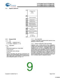
24 MHz
C1
C2
12 pf
12 pf
3.4
Buses
All packages: 8- or 16-bit “FIFO” bidirectional data bus, multi-
plexed on I/O ports B and D. 128-pin package: adds 16-bit
output-only 8051 address bus, 8-bit bidirectional data bus.
20 × PLL
12-pF capacitor values assumes a trace capacitance
of 3 pF per side on a four-layer FR4 PCA
Figure 3-1. Crystal Configuration
Note:
1. 115-KBaud operation is also possible by programming the 8051 SMOD0 or SMOD1 bits to a “1” for UART0 and/or UART1, respectively.
Document #: 38-08032 Rev. *K
Page 3 of 60
[+] Feedback

 CYPRESS [ CYPRESS ]