CY7C68013A, CY7C68014A
CY7C68015A, CY7C68016A
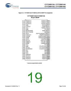
3. Pin Assignments
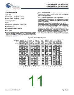
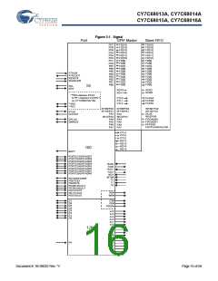
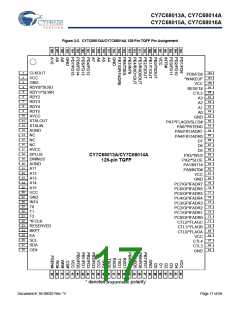
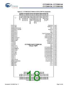
Figure 3-1 on page 16 identifies all signals for the five package
types. The following pages illustrate the individual pin diagrams,
plus a combination diagram showing which of the full set of
signals are available in the 128-pin, 100-pin, and 56-pin
packages.
The 128-pin package adds the 8051 address and data buses
plus control signals. Note that two of the required signals, RD#
and WR#, are present in the 100-pin version.
In the 100-pin and 128-pin versions, an 8051 control bit can be
set to pulse the RD# and WR# pins when the 8051 reads
from/writes to PORTC. This feature is enabled by setting
PORTCSTB bit in CPUCS register.
The signals on the left edge of the 56-pin package in Figure 3-1
on page 16 are common to all versions in the FX2LP family with
the noted differences between the CY7C68013A/14A and the
CY7C68015A/16A.
Section 9.5 displays the timing diagram of the read and write
strobing function on accessing PORTC.
Three modes are available in all package versions: Port, GPIF
master, and Slave FIFO. These modes define the signals on the
right edge of the diagram. The 8051 selects the interface mode
using the IFCONFIG[1:0] register bits. Port mode is the power on
default configuration.
The 100-pin package adds functionality to the 56-pin package by
adding these pins:
■ PORTC or alternate GPIFADR[7:0] address signals
■ PORTE or alternate GPIFADR[8] address signal and seven
additional 8051 signals
■ Three GPIF Control signals
■ Four GPIF Ready signals
■ Nine 8051 signals (two USARTs, three timer inputs, INT4,and
INT5#)
■ BKPT, RD#, WR#.
Document #: 38-08032 Rev. *V
Page 15 of 66

 CYPRESS [ CYPRESS ]