FOR
FOR
CY7C63411/12/13
CY7C63511/12/13
CY7C63612/13
3.0
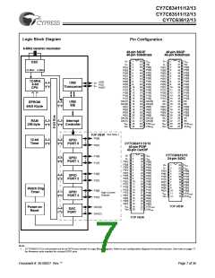
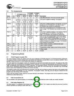
Pin Assignments
CY7C635 CY7C636
CY7C63411/12/13
11/12/13
48-Pin
1,2
12/13
24-Pin
1,2
Name
I/O
40-Pin
48-Pin
Description
D+, D–
I/O
1,2
1,2
USB differential data; PS/2 clock and data signals
GPIO port 0 capable of sinking 7 mA (typical)
P0[7:0]
15,26,16, 17,32,18, 17,32,18,
25,17,24, 31,19,30, 31,19,30,
7,18,8,
17,9,16,
10,15
I/O
I/O
I/O
I/O
18,23
20,29
20,29
P1[3:0]
P2
11,30,12, 11,38,12, 11,38,12,
29,13,28, 37,13,36, 37,13,36,
5,20,6,
19
GPIO Port 1 capable of sinking 7 mA (typical). P1[7:4] not
bonded out on CY7C63612/13. See note on page 17
for firmware code needed for unused pins.
14,27
14,35
14,35
7,34,8,
33,9,32,
10,31
7,42,8,
41,9,40,
10,39
7,42,8,
41,9,40,
10,39
n/a
GPIO Port 2 not bonded out on CY7C63612/13. See
note on page 17 for firmware code needed for unused
pins.
P3[7:4]
DAC
3,38,4,
37,5,36,
6,35
3,46,4,
45,5,44,
6,43
3,46,4,
45,5,44,
6,43
3,22,4,
21
GPIO Port 3 capable of sinking 12 mA (typical). P3[3:0]
not bonded out on CY7C63612/13. See note on
page 17 for firmware code needed for unused pins.
I/O
n/a
n/a
15,34,16,
33,21,28,
22,27
n/a
DAC I/O Port with programmable current sink outputs.
DAC[1:0] offer a programmable range of 3.2 to 16 mA
typical. DAC[7:2] have a programmable sink current
range of 0.2 to 1.0 mA typical. DAC I/O Port not bonded
out on CY7C63612/13. See note on page 17 for firmware
code needed for unused pins.
XTALIN
IN
21
22
25
26
25
26
13
14
6-MHz ceramic resonator or external clock input
6-MHz ceramic resonator
XTALOUT OUT
VPP
VCC
Vss
19
23
23
11
Programming voltage supply, ground during operation
Voltage supply
40
48
48
24
20,39
24,47
24,47
12,23
Ground
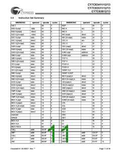
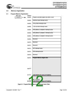
4.0
4.1
Programming Model
14-bit Program Counter (PC)
The 14-bit Program Counter (PC) allows access for up to 8 kilobytes of EPROM using the CY7C634XX/5XX/6XX architecture.
The program counter is cleared during reset, such that the first instruction executed after a reset is at address 0x0000h. This is
typically a jump instruction to a reset handler that initializes the application.
The lower eight bits of the program counter are incremented as instructions are loaded and executed. The upper six bits of the
program counter are incremented by executing an XPAGE instruction. As a result, the last instruction executed within a 256-byte
“page” of sequential code should be an XPAGE instruction. The assembler directive “XPAGEON” will cause the assembler to
insert XPAGE instructions automatically. As instructions can be either one or two bytes long, the assembler may occasionally
need to insert a NOP followed by an XPAGE for correct execution.
The program counter of the next instruction to be executed, carry flag, and zero flag are saved as two bytes on the program stack
during an interrupt acknowledge or a CALL instruction. The program counter, carry flag, and zero flag are restored from the
program stack only during a RETI instruction.
Please note the program counter cannot be accessed directly by the firmware. The program stack can be examined by reading
SRAM from location 0x00 and up.
4.2
8-bit Accumulator (A)
The accumulator is the general purpose, do everything register in the architecture where results are usually calculated.
4.3
8-bit Index Register (X)
The index register “X” is available to the firmware as an auxiliary accumulator. The X register also allows the processor to perform
indexed operations by loading an index value into X.
Document #: 38-08027 Rev. **
Page 8 of 36

 CYPRESS [ CYPRESS ]