ADVANCE
CYW43570
Document History
Document Title: CYW43570 Single-Chip 5G WiFi IEEE 802.11ac 2×2 MAC/Baseband/Radio with Integrated Bluetooth 4.1
and EDR
Document Number: 002-15054
Orig. of
Change
Submission
Date
Revision
ECN
Description of Change
**
–
–
04/02/2014 43570-DS100-R
Initial release
*A
*B
–
–
–
04/14/2014 43570-DS101-R
Updated:
• Section 22. Ordering Information
–
–
–
07/02/2014 43570-DS102-R
Updated:
• Table 18. Pin List
• Table 19. Signal Descriptions
*C
*D
–
–
07/11/2014 43570-DS103-R
Updated:
• Table 37. Typical WLAN Power Consumption
• Table 38. Bluetooth BLE and FM Current Consumption
07/29/2014 43570-DS104-R
Updated:
• Table 5. Power Control Pin Description
• Figure 5. Startup Signaling Sequence
• Table 6. SPI-to-UART Signal Mapping
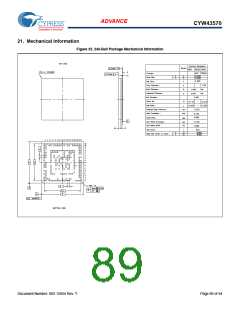
• Figure 32. 242-Ball Package Mechanical Information
• PCM Interface Timing
• Table 15. UART Timing Specifications
• Figure 16. UART Timing
• Figure 32. 242-Ball Package Mechanical Information
Added:
• Table 6. PCM-to-Serial Flash Interface Mapping
*E
–
–
08/03/2015 43570-DS105-R
Updated:
• General Description and Features
• Figure 1. Functional Block Diagram for PCIe (WLAN) and BT (USB 2.0) Interfaces
• Table 2. Device Interface Support
• Figure 2. CYW43570/E Block Diagram
• CYW43570/E PMU Features
• UART/USB Transport Detection
• USB Interface
• Table 17. Strapping Options PCIe
• Table 20. BT GPIO Functions and Strapping Options
• Table 24. Bluetooth Receiver RF Specifications
• Table 28. 2.4 GHz Band General RF Specifications
• Table 29. WLAN 2.4 GHz Receiver Performance Specifications through
Table 32. WLAN 5 GHz Transmitter Performance Specifications
• Table 37. Typical WLAN Power Consumption
• Table 38. Bluetooth Current Consumption
• Bluetooth Current Consumption
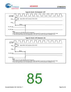
• Figure 26. WLAN = ON, Bluetooth = ON
• Figure 27. WLAN = OFF, Bluetooth = OFF
• Figure 28. WLAN = ON, Bluetooth = OFF
• Figure 29. WLAN = OFF, Bluetooth = ON
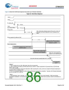
• Figure 30. WLAN Boot Sequence
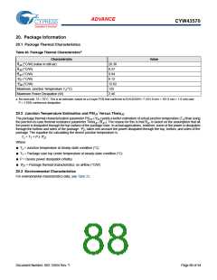
• Table 40. Package Thermal Characteristics
Added:
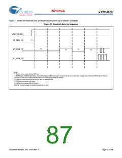
• Figure 31. Bluetooth Boot-Up Sequence
• Note: VBAT is the main power supply (ranges from 3.0V to 3.6V) to the chip.
*F
–
–
01/05/2016 43570-DS106-R
Updated:
• Figure 1. Functional Block Diagram for PCIe (WLAN) and BT (USB 2.0) Interfaces
• SPI/UART Transport Detection
Document Number: 002-15054 Rev. *I
Page 91 of 93

 CYPRESS [ CYPRESS ]