BCM4339 Preliminary Data Sheet
Interface Timing and AC Characteristics
Section 20: Interface Timing and AC
Characteristics
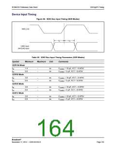
SDIO/gSPI Timing
SDIO Default Mode Timing
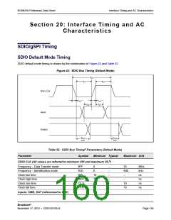
SDIO default mode timing is shown by the combination of Figure 43 and Table 52.
Figure 43: SDIO Bus Timing (Default Mode)
fPP
tWL
tWH
SDIO_CLK
tTHL
tTLH
tIH
tISU
Input
Output
tODLY
tODLY
(max)
(min)
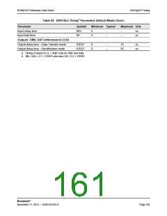
Table 52: SDIO Bus Timinga Parameters (Default Mode)
Parameter
Symbol
Minimum Typical
Maximum Unit
SDIO CLK (All values are referred to minimum VIH and maximum VILb)
Frequency – Data Transfer mode
Frequency – Identification mode
Clock low time
fPP
0
–
–
–
–
–
–
25
400
–
MHz
kHz
ns
fOD
tWL
tWH
tTLH
tTHL
0
10
10
–
Clock high time
–
ns
Clock rise time
10
10
ns
Clock fall time
–
ns
Inputs: CMD, DAT (referenced to CLK)
Broadcom®
November 17, 2014 • 4339-DS106-R
Page 159

 CYPRESS [ CYPRESS ]