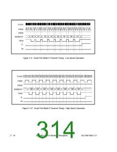
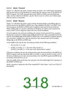
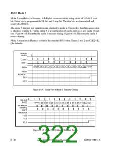
C.3.3.2 Mode 1 Transmit
Figure C-11. illustrates the mode 1 transmit timing. In mode 1, the UART begins transmitting
after the first roll over of the divide-by-16 counter after the software writes to the SBUF0 (or
SBUF1) register. The UART transmits data on the TXD0 (or TXD1) pin in the following
order: start bit, 8 data bits (LSB first), stop bit. The TI_0 (or TI_1) bit is set 2 CLK24 cycles
after the stop bit is transmitted.
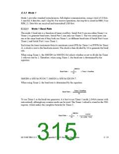
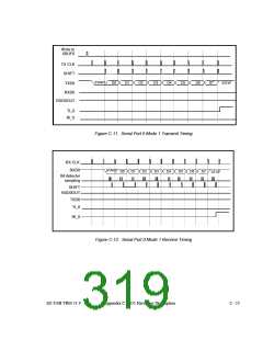
C.3.3.3 Mode 1 Receive
Figure C-12. illustrates the mode 1 receive timing. Reception begins at the falling edge of a
start bit received on the RXD0 (or RXD1) pin, when enabled by the REN_0 (or REN_1) bit.
For this purpose, the RXD0 (or RXD1) pin is sampled 16 times per bit for any baud rate.
When a falling edge of a start bit is detected, the divide-by-16 counter used to generate the
receive clock is reset to align the counter roll over to the bit boundaries.
For noise rejection, the serial port establishes the content of each received bit by a majority
decision of 3 consecutive samples in the middle of each bit time. This is especially true for the
start bit. If the falling edge on the RXD0 (or RXD1) pin is not verified by a majority decision
of 3 consecutive samples (low), then the serial port stops reception and waits for another
falling edge on the RXD0 (or RXD1) pin.
At the middle of the stop bit time, the serial port checks for the following conditions:
•
•
RI_0 (or RI_1) = 0, and
If SM2_0 (or SM2_1) = 1, the state of the stop bit is 1.
(If SM2_0 (or SM2_1) = 0, the state of the stop bit doesn’t matter.)
If the above conditions are met, the serial port then writes the received byte to the SBUF0 (or
SBUF1) register, loads the stop bit into RB8_0 (or RB8_1), and sets the RI_0 (or RI_1) bit. If
the above conditions are not met, the received data is lost, the SBUF register and RB8 bit are
not loaded, and the RI bit is not set.
After the middle of the stop bit time, the serial port waits for another high-to-low transition on
the (RXD0 or RXD1) pin.
Mode 1 operation is identical to that of the standard 8051 when Timers 1 and 2 use CLK24/12
(the default).
C - 22
Appendix C: 8051 Hardware Description
EZ-USB TRM v1.9

 CYPRESS [ CYPRESS ]