Wireless Modem Data Pump
FX909A
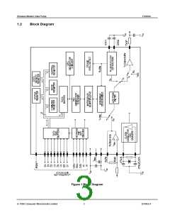
1.3
Signal List
Package
D2/D5/P4
Signal
Description
Pin No.
Name
Type
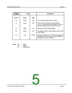
1
IRQN
O/P
A 'wire-ORable' output for connection to the host
mC's Interrupt Request input. This output has a
low impedance pull down to V when active
SS
and is high impedance when inactive.
2
3
4
5
6
7
8
9
D7
D6
D5
D4
D3
D2
D1
D0
BI
BI
BI
BI
BI
BI
BI
BI
)
)
)
)
)
)
)
)
8-bit bidirectional 3-state mC interface data
lines.
10
RDN
I/P
Read. An active low logic level input used to
control the reading of data from the modem into
the host mC.
11
WRN
I/P
Write. An active low logic level input used to
control the writing of data into the modem from
the host mC.
12
13
V
Power
I/P
The negative supply rail (ground).
ss
CSN
Chip Select. An active low logic level input to the
modem, used to enable a data read or write
operation.
14
15
A0
A1
I/P
I/P
)
)
Two logic level modem register select
inputs.
16
17
XTALN
O/P
I/P
The output of the on-chip oscillator.
XTAL/CLOCK
The input to the on-chip oscillator, for external
Xtal circuit or clock.
18
19
DOC 2
DOC 1
O/P
O/P
)
)
)
Connections to the Rx level measurement
circuitry. A capacitor should be connected
from each pin to V
SS.
ã 1996 Consumer Microcircuits Limited
4
D/909A/4

 CMLMICRO [ CML MICROCIRCUITS ]