Evaluation Kit for CMX990
EV9900A
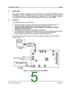
4.
Signal Lists
CONNECTOR PINOUT
Connector
Connector
Pin No.
Signal
Name
Signal
Type
Description
Ref.
J1
N/A
REFIN
RF / Clock Clock input / output. By selecting coupling
capacitors (C3 / C4) this port may be used to
monitor the on-board 14.4MHz reference or the
external reference input.
J2
J3
N/A
N/A
RXIN1
RXIN2
RF
RF
Input to receiver LNA.
By selecting components this port may be used
as an LNA output or input to the receiver mixer.
NB: This port is a test port (solder pads)
designed to allow connection of a coax cable.
J4
J5
N/A
N/A
IFOUT
IF IN
RF
RF
1st Mixer Output or input to IF filter (F2).
Output of IF filter (F2) or input to CMX990
receiver IF stages.
J6
J7
N/A
N/A
N/A
N/A
N/A
N/A
TXI
TXQ
BASEBAND EV9900A is not configured to use this port.
BASEBAND EV9900A is not configured to use this port.
J8
TX VCO O/P
TXOUT
RF
RF
RF
RF
Monitor point for Tx VCO feedback signal.
400MHz / 800MHz transmitter output.
J9
J10
J11
MAIN LO
AUX LO
Input or output / monitor for main local oscillator.
Input or output / monitor for auxiliary (180MHz)
local oscillator (normally not connected).
J12
J12
J12
J13
3
+7.2V
+3.5V
DC
DC
7.2V power supply input.
2
1
3.5V power supply for RF power amplifier.
Power supply ground.
GND
DC
1 – 40
HOST
LOGIC
8 bit parallel interface from CMX990 to host /
controller or PC. See schematics and CMX990
datasheet for details.
INTERFACE
J14
J15
J15
J15
J15
J15
J16
J17
1 – 8
TX/RX/I/Q
TX/RX/I/Q
DAC3
BASEBAND EV9900A is not configured to use this port.
BASEBAND EV9900A is not configured to use these pins.
BASEBAND DAC3 output.
1,3,5,7
2
4
DAC2
BASEBAND DAC2 output.
6
ADC5
BASEBAND ADC5 input.
8
ADC4
BASEBAND ADC4 input.
VOID
N/A
VOID
N/A
N/A
Void
N/A
EV9900A is not configured to use this
connector.
J18
N/A
RF_ANT
RF
TX / RX Switch Output (Default configuration of
EV9900A does not use this connector).
Table 1 – Signal List
© 2007 CML Microsystems Plc
9
UM9900A/3

 CMLMICRO [ CML MICROCIRCUITS ]