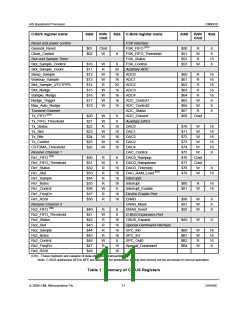
AIS Baseband Processor
CMX910
C-BUS register name
Addr
R/W/
Cmd
Size C-BUS register name
Addr
R/W/
Cmd
Size
Reset and power control
General_Reset
Clock_Control
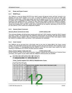
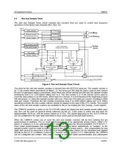
Slot and Sample Timer
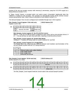
Slot_Sample_Control
Slot_Sample_Count
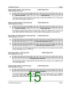
Sleep_Sample
Wakeup_Sample
Slot_Sample_UTC1PPS
Slot_Nudge
FSK Interface
$01
$02
Cmd
W
-
FSK_FIFO (DS)
FSK_FIFO_Threshold
FSK_Status
FSK_Control
Auxiliary ADC
ADC0
$50
$51
$52
$53
R
W
R
8
8
8
16
8
$10
$11
$12
$13
$14
$15
$16
$17
$18
W
R
8
W
32
16
16
32
16
16
16
16
W
W
R
$60
$61
$62
$63
$64
$65
$66
$67
$68
R
R
16
16
16
16
16
8
ADC1
ADC2
R
W
W
W
W
ADC3
R
Sample_Nudge
Nudge_Trigger
Max_Auto_Nudge
Transmit Channel
Tx_FIFO (DS)
ADC4
R
ADC_Control1
ADC_Control2
ADC_Status
ADC_Convert
Auxiliary DACs
DAC0
W
W
R
8
8
$20
$21
$22
$23
$24
$25
$26
W
W
R
8
Cmd
-
Tx_FIFO_Threshold
Tx_Status
8
16
16
16
16
16
$70
$71
$72
$73
$74
$75
$76
$77
$78
$79
W
W
16
16
16
16
16
8
Tx_Slot
W
W
W
W
DAC1
Tx_Bits
DAC2
W
Tx_Control
DAC2
W
CSTDMA_Threshold
Receive Channel 1
Rx1_FIFO (DS)
Rx1_FIFO_Threshold
Rx1_Status
DAC4
W
DAC_Control
DAC0_Rampup
DAC0_Rampdown
DAC0_Timestep
DAC_RAM_Load (DS)
Interrupts
W
$30
$31
$32
$33
$34
$35
$36
$37
$38
R
W
R
R
R
R
W
R
R
8
Cmd
Cmd
W
-
8
-
16
16
16
16
8
8
Rx1_Slot
W
16
Rx1_Sample
Rx1_Bytes
Interrupt
$80
$81
R
16
16
Rx1_Control
Interrupt_Enable
Device Enable Port
ENAB
W
Rx1_FreqErr
16
16
Rx1_RSSI
$90
$91
$92
W
W
W
8
8
8
Receive Channel 2
Rx2_FIFO (DS)
Rx2_FIFO_Threshold
Rx2_Status
ENAB_Mask
ENAB_Invert
C-BUS Expansion Port
CBUS_Expand
Special Command Interface
SPC_In0
$40
$41
$42
$43
$44
$45
$46
$47
$48
R
W
R
R
R
R
W
R
R
8
8
16
16
16
16
8
$A0
W
8
Rx2_Slot
Rx2_Sample
$B0
$B1
$B2
$B4
W
W
R
16
16
16
8
Rx2_Bytes
SPC_In1
Rx2_Control
SPC_Out0
Rx2_FreqErr
16
16
Special_Command
W
Rx2_RSSI
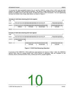
(DS) - These registers are capable of data-streaming transactions.
Note: C-BUS addresses $F0 to $FE are allocated for production testing and should not be accessed in normal operation.
Table 1 Summary of C-BUS Registers
© 2009 CML Microsystems Plc
11
D/910/6

 CMLMICRO [ CML MICROCIRCUITS ]