AIS Baseband Processor
CMX910
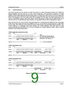
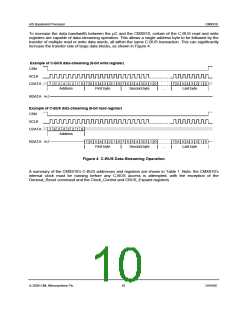
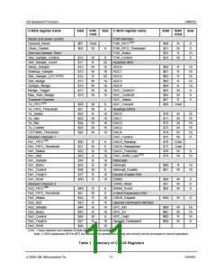
To increase the data bandwidth between the µC and the CMX910, certain of the C-BUS read and write
registers are capable of data-streaming operation. This allows a single address byte to be followed by the
transfer of multiple read or write data words, all within the same C-BUS transaction. This can significantly
increase the transfer rate of large data blocks, as shown in Figure 4.
Example of C-BUS data-streaming (8-bit write register)
CSN
SCLK
CDATA
7 6 5 4 3 2 1 0 7 6 5 4 3 2 1 0 7 6 5 4 3 2 1 0
7 6 5 4 3 2 1 0
Last byte
Address
First byte
Second byte
…
Hi-Z
RDATA
Example of C-BUS data-streaming (8-bit read register)
CSN
SCLK
CDATA
7 6 5 4 3 2 1 0
Address
Hi-Z
RDATA
7 6 5 4 3 2 1 0 7 6 5 4 3 2 1 0
7 6 5 4 3 2 1 0
Last byte
First byte
Second byte
…
Figure 4 C-BUS Data-Streaming Operation
A summary of the CMX910’s C-BUS addresses and registers are shown in Table 1. Note: the CMX910’s
internal clock must be running before any C-BUS access is attempted, with the exception of the
General_Reset command and the Clock_Control and CBUS_Expand registers.
© 2009 CML Microsystems Plc
10
D/910/6

 CMLMICRO [ CML MICROCIRCUITS ]