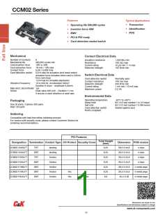
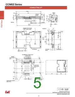
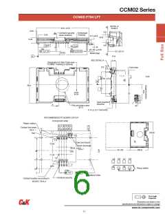
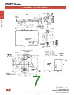
CCM02 Series
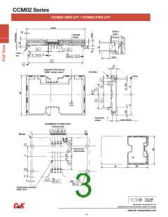
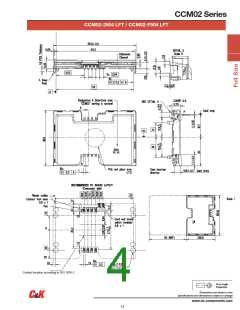
CCM02-F844a LFT / CCM02-F844b LFT
0,2±0,1
DETAIL B
Scale 5
58±0,3
0,7
2,05
Embossed
Channel
(14x) 1
0,3
A
0,2±0,15
18,87
(5x)
2,54
metal peg
(4x)
0,05
Ø
1,62
±
51,5
Ø 0.2
A
B
A-A
6
A
Card stop
SEE DETAIL B
A
Labelling : Designation &
Date-Code area
F844T
xx xx
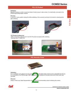
Contacts security
(closed position)
A
3,6±0,3
Card entry
45º
RECOMMENDED PC BOARD LAYOUT
(Component side)
C6
C8
C5
C7
Contact foot area
P4
P3
P2
P1
metallized holes
Card end travel
switch terminals
11,3
\Piracy\
38,8
(4x)
Ø 1,9
A
switch
Ø
0,1
SW
SW
C1 C2 C3 C4
14
Scale 1
1,27
Card insertion
direction
P2
P4
P3
0
1,27
P1
(6x) 1,5
0,05
C5 C6 C7 C8
Protection cover
terminals
Plastic
outline
(50)
(40,5)
20
1,3
0,2
Contact location
according to ISO/IEC 7816-2
Please don't apply any solder
paste on these 4 pads
Dimensions are shown in mm
Specifications and dimensions subject to change
www.ck-components.com
18

 CK-COMPONENTS [ C&K COMPONENTS ]