CS49300 Family DSP
of integration, many of these pins are internally
multiplexed to serve multiple purposes. Some pins
are designed to operate in one mode at power up,
and serve a different purpose when the DSP is
running. Other pins have functionality which can
be controlled by the application running on the
DSP. In order to better explain the behavior of the
part, the pins which are multiplexed have been
given multiple names. Each name is specific to the
pin’s operation in a particular mode.
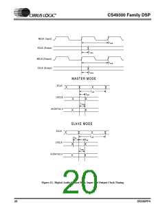
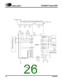
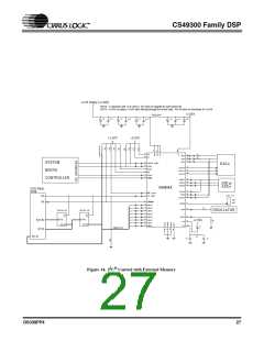
3. TYPICAL CONNECTION
DIAGRAMS
Six typical connection diagrams have been
presented to illustrate using the part with the
different communication modes available. They
are as follows:
2 ®
Figure 13, "I C Control" on page 26
2 ®
Figure 14, "I C Control with External Memory"
on page 27
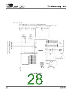
Figure 15, "SPI Control" on page 28
Figure 16, "SPI Control with External Memory" on
page 29
An example of this would be the use of pin 20 in
one of the serial control modes. During the boot
period of the CS493XX, pin 20 is called ABOOT.
ABOOT is sampled on the rising edge of RESET.
If ABOOT is high the host must download code to
the DSP. If ABOOT is low when sampled, the
CS493XX goes into autoboot mode and loads itself
with code by generating addresses and reading data
on EMAD[7:0]. When the part has been loaded
with code and is running an application, however,
pin 20 is called INTREQ. INTREQ is an open drain
output used to inform the host that the DSP has an
outgoing message which should be read.
®
Figure 17, "Intel Parallel Control Mode" on page
30
®
Figure 18, "Motorola Parallel Control Mode" on
page 31
The following should be noted when viewing the
typical connection diagrams:
The pins are grouped functionally in each of the
typical connection diagrams. Please be aware that
the CS493XX symbol may appear differently in
each diagram.
The external memory interface is only supported
In this document, pins will be referred to by their
when a serial communication mode has been functionality. Section 12, “Pin Descriptions” on
chosen.
page 80 describes each pin of the CS493XX and
lists all of its names. Please refer to this section
when exact pin numbers are in question.
The typical connection diagrams demonstrate the
PLL being used (CLKSEL is pulled low). To use
CLKIN as the DSP clock, CLKSEL should be
pulled high. The system designer must be aware
that certain software features may not be available
if external CLKIN is used as the DSP must run
slower when external CLKIN is used. The system
designer should also be aware of additional duty
cycle requirements when using external CLKIN as
a DSP clock. It is highly suggested that the system
designer use the PLL and pull CLKSEL low.
The part has 12 general purpose input and output
(GPIO[11:0]) pins that all have multiple
functionality. While in one of the parallel
communication modes (Section 6.2, “Parallel Host
Communication” on page 41), these pins are used
to implement the parallel host communication
interface. While in one of the serial host modes
these pins are used to implement an external
memory interface. Alternatively while in one of the
serial host modes these pins could be used for
another general purpose if the application code has
been programmed to support the special purpose.
In this document the pins are referenced by the
3.1. Multiplexed Pins
The CS493XX family of digital signal processors
(DSPs) incorporate a large amount of flexibility
into a 44 pin package. Because of the high degree
24
DS339PP4

 CIRRUS [ CIRRUS LOGIC ]